3.3.33 Tx Buffer Configuration Register (M_CAN_TXBC)
NOTE
Be aware that the sum of TFQS and NDTB may be not greater
than 32. There is no check for erroneous configurations. The Tx
Buffers section in the Message RAM starts with the dedicated
Tx Buffers.
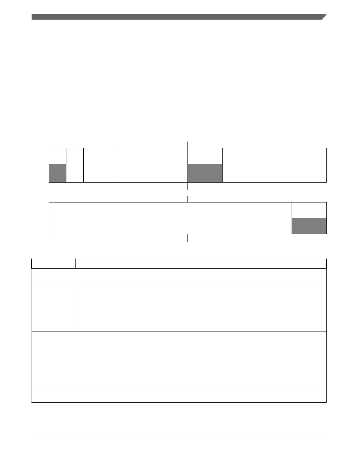
Address: 0h base + C0h offset = C0h
Bit 0 1 2 3 4 5 6 7 8 9 10 11 12 13 14 15
R
0
TFQM
TFQS
0
NDTB
W
Reset
0 0 0 0 0 0 0 0 0 0 0 0 0 0 0 0
Bit
16 17 18 19 20 21 22 23 24 25 26 27 28 29 30 31
R
TBSA
0
W
Reset
0 0 0 0 0 0 0 0 0 0 0 0 0 0 0 0
M_CAN_TXBC field descriptions
Field Description
0
Reserved
This field is reserved.
This read-only field is reserved and always has the value 0.
1
TFQM
Tx FIFO/Queue Mode
NOTE: This field has Protected Write status.
0 Tx FIFO operation
1 Tx Queue operation
2–7
TFQS
Transmit FIFO/Queue Size
NOTE: This field has Protected Write status.
0 No Tx FIFO/Queue
1-32 Number of Tx Buffers used for Tx FIFO/Queue
>32 Values greater than 32 are interpreted as 32
8–9
Reserved
This field is reserved.
This read-only field is reserved and always has the value 0.
Table continues on the next page...
Chapter 3 Modular CAN (M_CAN)
MPC5777C Reference Manual Addendum, Rev. 1, 12/2015
Freescale Semiconductor, Inc. 69

 Loading...


