271
Timer and Counter Instructions Section 3-6
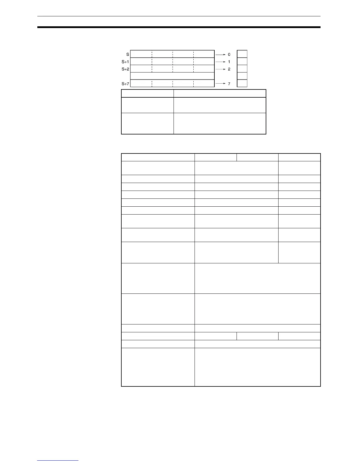
Note S through S+7 must be in the same data area.
Operand Specifications
Description When the execution condition for MTIM(543)/MTIMX(554) is ON and the reset
and timer bits are both OFF, MTIM(543)/MTIMX(554) increments the PV in
D2. If the pause bit is turned ON, the timer will stop incrementing the PV, but
the PV will retain its value. MTIM(543)/MTIMX(554) will resume timing when
the pause bit goes OFF again.
Data Range
BCD One word for each of 8 timer SV:
#0000 to #9999
Binary One word for each of 8 timer SV:
&0 to &65535 (decimal)
#0000 to #FFFF (hex)
Corresponding bit
(Completion Flag) in D1
Area D1 D2 S
CIO Area CIO 0000 to CIO 6143 CIO 0000 to
CIO 6136
Work Area W000 to W511 W000 to W504
Holding Bit Area H000 to H511 H000 to H504
Auxiliary Bit Area A448 to A959 A000 to A952
Timer Area T0000 to T4095 T0000 to T4088
Counter Area C0000 to C4095 C0000 to C4088
DM Area D00000 to D32767 D00000 to
D32760
EM Area without bank E00000 to E32767 E00000 to
E32760
EM Area with bank En_00000 to En_32767
(n = 0 to C)
En_00000 to
En_32760
(n = 0 to C)
Indirect DM/EM addresses in
binary
@ D00000 to @ D32767
@ E00000 to @ E32767
@ En_00000 to @ En_32767
(n = 0 to C)
Indirect DM/EM addresses in
BCD
*D00000 to *D32767
*E00000 to *E32767
*En_00000 to *En_32767
(n = 0 to C)
Constants ---
Data Registers --- DR0 to DR15 ---
Index Registers ---
Indirect addressing using
Index Registers
,IR0 to ,IR15
–2048 to +2047 ,IR0 to –2048 to +2047 ,IR15
DR0 to DR15, IR0 to IR15
,IR0+(++) to ,IR15+(++)
,–(– –)IR0 to, –(– –)IR15