723
Table Data Processing Instructions Section 3-17
Note R1 and R1+C–1 must be in the same data area.
Operand Specifications
Description SRCH(181) searches the range of memory from R1 to R1+C–1 for words that
contain the comparison data (Cd). If a match is found, SRCH(181) writes the
PLC memory address of the word to IR00 and turns the Equals Flag ON.
(If there are two or more matches, just the address of the first word containing
the comparison data is written to IR00.)
When bit 15 of C+1 has been set to 1, SRCH(181) writes the number of
matches to DR00. When bit 15 of C+1 is 0, DR00 is left unchanged.
Area C R1 Cd
CIO Area CIO 0000 to
CIO 6142
CIO 0000 to CIO 6143
Work Area W000 to W510 W000 to W511
Holding Bit Area H000 to H510 H000 to H511
Auxiliary Bit Area A000 to A958 A000 to A959
Timer Area T0000 to T4094 T0000 to T4095
Counter Area C0000 to C4094 C0000 to C4095
DM Area D00000 to
D32766
D00000 to D32767
EM Area without bank E00000 to
E32766
E00000 to E32767
EM Area with bank En_00000 to
En_32766
(n = 0 to C)
En_00000 to En_32767 (n = 0 to C)
Indirect DM/EM
addresses in binary
@ D00000 to @ D32767
@ E00000 to @ E32767
@ En_00000 to @ En_32767
(n = 0 to C)
Indirect DM/EM
addresses in BCD
*D00000 to *D32767
*E00000 to *E32767
*En_00000 to *En_32767
(n = 0 to C)
Constants Specified values
only
--- #0000 to #FFFF
(binary)
Data Registers --- DR0 to DR15
Index Registers ---
Indirect addressing
using Index Registers
,IR0 to ,IR15
–2048 to +2047 ,IR0 to –2048 to +2047 ,IR15
DR0 to DR15, IR0 to IR15
,IR0+(++) to ,IR15+(++)
,–(– –)IR0 to, –(– –)IR15
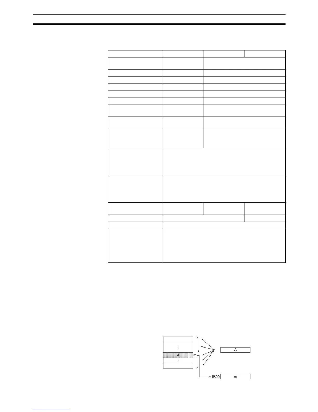
R1+(C–1)
C
R1 Search
Match
Cd
PC memory
address