788
Data Control Instructions Section 3-18
R: Pulse Output Bit
Specifies the destination output bit for the pulse output.
Normally, specify an output bit allocated to a Transistor Output Unit and con-
nect a solid state relay to the Transistor Output Unit.
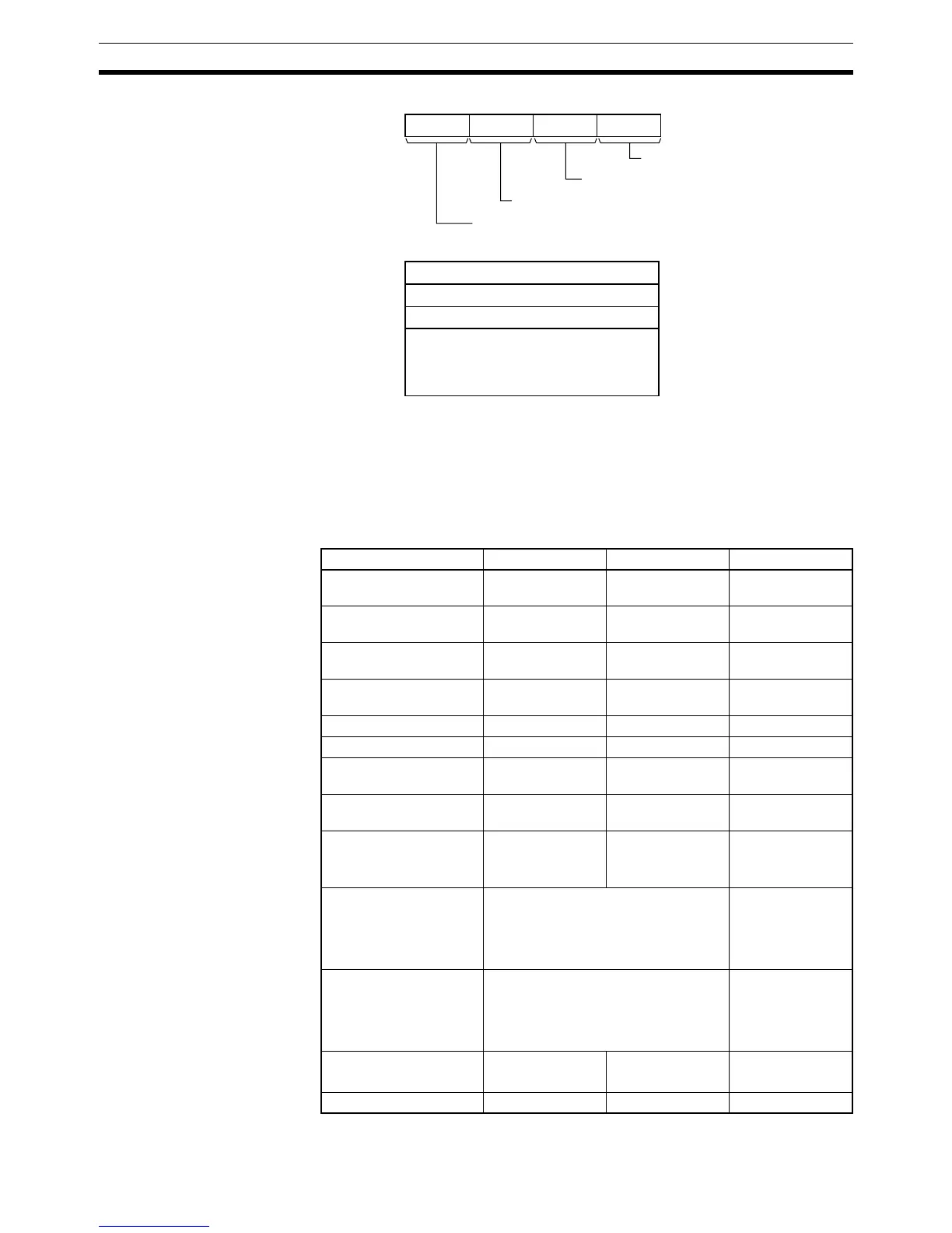
Operand Specifications
C+1
C+2
C+3
C+4
C+5
C+6
015
C
815 1211 0347
Manipulated variable range
Input type
Input read timing
Output limit function
Note: For details, see the description of each parameter.
Control period
Output lower limit
Output upper limit
Work area
(3 words, cannot be used by user)
Area S C R
CIO Area CIO 0000 to
CIO 6143
CIO 0000 to
CIO 6137
CIO 000000 to
CIO 614315
Work Area W000 to W511 W000 to W505 W00000 to
W51115
Holding Bit Area H000 to H511 H000 to H505 H00000 to
H51115
Auxiliary Bit Area A000 to 959 A000 to A953 A44800 to
A95915
Timer Area T0000 to T4095 T0000 to T4089 ---
Counter Area C0000 to C4095 C0000 to C4089 ---
DM Area D00000 to
D32767
D00000 to
D32761
---
EM Area without bank E00000 to
E32767
E00000 to
E32761
---
EM Area with bank En_00000 to
En_32767
(n = 0 to C)
En_00000 to
En_32761
(n = 0 to C)
---
Indirect DM/EM
addresses in binary
@ D00000 to @ D32767
@ E00000 to @ E32767
@ En_00000 to @ En_32767
(n = 0 to C)
---
Indirect DM/EM
addresses in BCD
*D00000 to *D32767
*E00000 to *E32767
*En_00000 to *En_32767
(n = 0 to C)
---
Constants #0000 to #FFFF
(binary)
--- ---
Data Registers DR0 to DR15 --- ---