GR740-UM-DS, Nov 2017, Version 1.7 450 www.cobham.com/gaisler
GR740
39.5.12 PCI interface timing
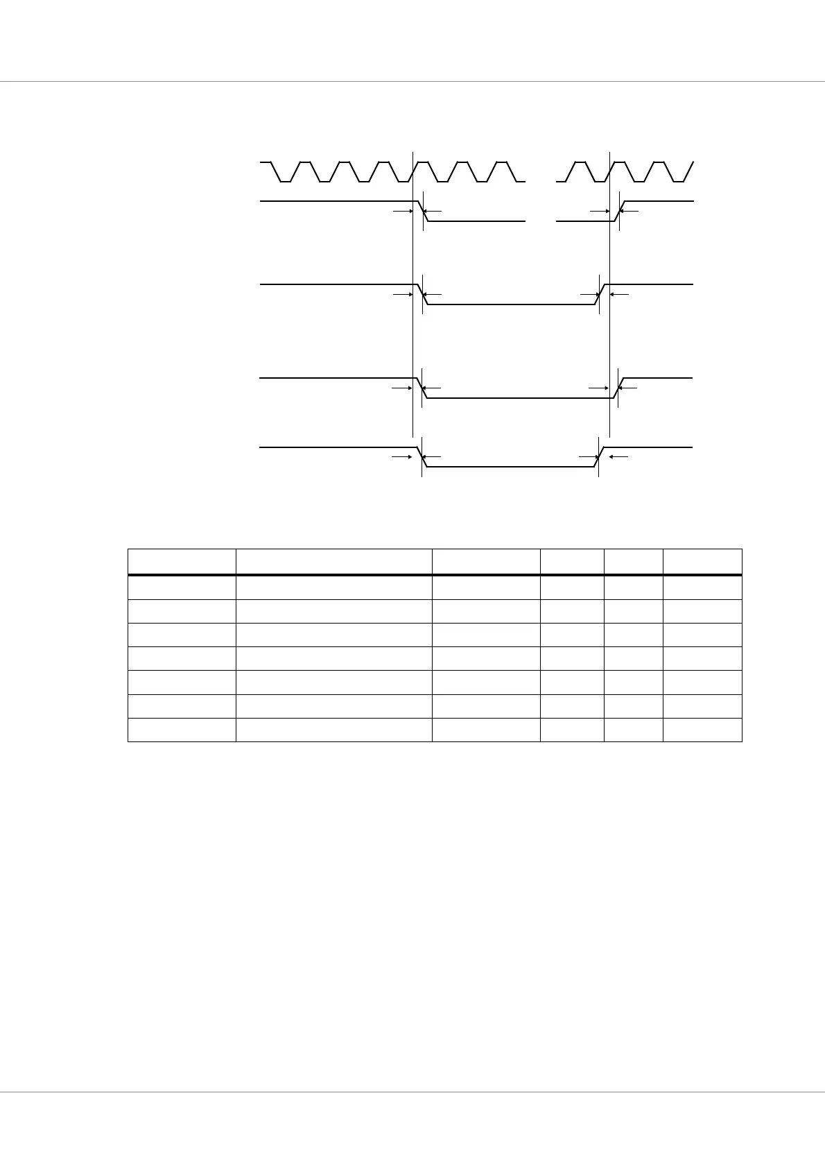
The timing waveforms and timing parameters are shown in figure 65 and are defined in table 589.
Table 589.Timing parameters
Name Parameter Reference edge Min Max Unit
t
PCICLK0
PCI clock period -
15, 30
-ns
t
PCI0
clock to output delay rising pci_clk edge 3.05
12.78
ns
t
PCI1
input to clock hold rising pci_clk edge 1.03 - ns
t
PCI2
input to clock setup rising pci_clk edge
6.44
-ns
t
PCI3
clock to output delay rising pci_clk edge 3.05
17.91
ns
t
PCI4
input to clock hold rising pci_clk edge 1.03 - ns
t
PCI5
input to clock setup rising pci_clk edge
6.44
-ns
Figure 65. Timing waveforms
t
PCI0
pci_ad[ ], pci_cbe[ ],
pci_clk
t
PCI0
t
PCI1
t
PCI2
t
PCI3
pci_gnt, pci_req
t
PCI3
t
PCI4
pci_gnt, pci_req
t
PCI5
pci_frame, pci_irdy,
pci_trdy, pci_stop,
pci_idsel, pci_devsel,
pci_perr, pci_serr,
pci_par, pci_int
pci_ad[ ], pci_cbe[ ],
pci_frame, pci_irdy,
pci_trdy, pci_stop,
pci_idsel, pci_devsel,
pci_perr, pci_serr,
pci_par