250
Intel
®
855GME Chipset and Intel
®
6300ESB ICH Embedded Platform Design Guide
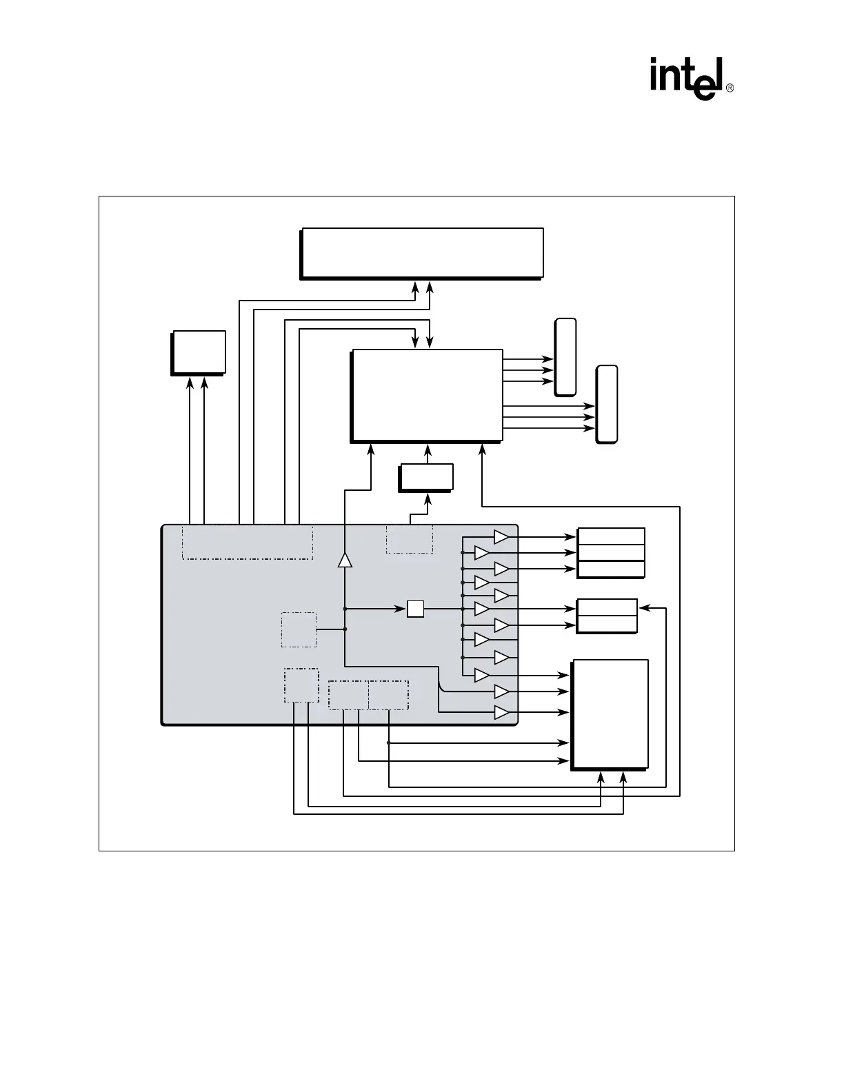
Platform Clock Routing Guidelines
Figure 137 depicts the system clock subsystem including the clock generator, major platform
components, and all the related clock interconnects.
Figure 137. Clock Distribution Diagram
B1364-01
CPU
ITP
USBCLK
CLK14
CLK66
CLK66
CLK33
Intel
®
855GME
Chipset
CK409
Intel
®
6300ESB
I/O
Controller
Intel
®
855GME
Chipset Clock
Distribution
100
MHz
66
MHz
48 MHz
PLL
SSCCLK
100 MHz Outputs
14 MHz
PLL
CLK33
PCICLK
DOTCLK
DDRCLKs
CLK66
SSCCLK
DDR Clocks
Differential Pairs
(100/133 MHz)
Low Voltage Differential Clocks
100 MHz Debug Hostclock
PCICLK
PCICLK
SSC
100 MHz CPU Hostclock
100 MHz MCH Hostclock
FWH
CLK33
SIO
PCI Slot0
PCI Slot1
PCI Slot2
/2
D
I
M
M
D
I
M
M