CONNECTORS AND JUMPERS MAINBOARD
5-2
Jumpers
See the following figure and table for information on mainboard jumpers.
\
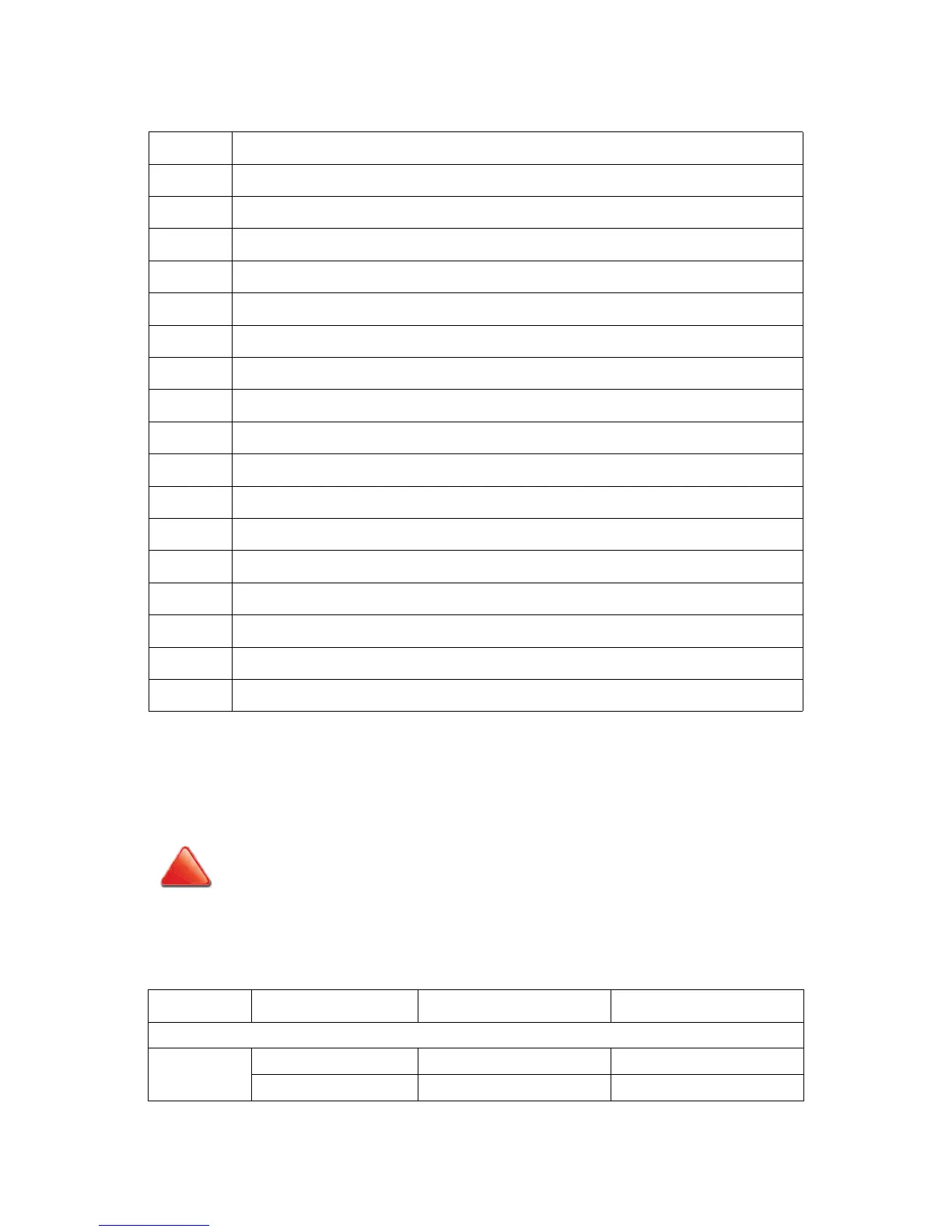
10 Reset button
11 Power button
12 AHCI SATA 2, 3, 4, 5 connectors
13 SCU0 SAS 0, 1, 2, 3 connector
14 SCU1 SAS 4, 5, 6, 7 connector
15 Internal USB connector
16 HDD power connectors for AHCI SATA and SCU SAS (12, 13, 14)
17 BIOS Socket
18 Mezzanine Connector
19 Upgrade ROM connector
20 RJ45
21 Battery connector
22 PCIe x 16 connector
23 CPLD
24 PCH chipset
25 Clock generator and clock buffer
26 Intel 82574 GB E LAN
CMOS Clear jumper - Clears NVRAM. The NVRAM will be cleared when the jumper is moved
over with the system powered off while still connected to power.
Pins 1-2: clears NVRAM
Pins 2-3: normal operation.
Table 2: Mainboard Jumpers
LOCATION JUMPER POSITIONS (PIN)FUNCTION DEFAULT SETTING
CMOS Clear
J43
1-2 Normal RTC RST x
2-3 CLR RTC Registers
Table 1: Mainboard Connectors (Continued)
LOCATION DESCRIPTION
 Loading...