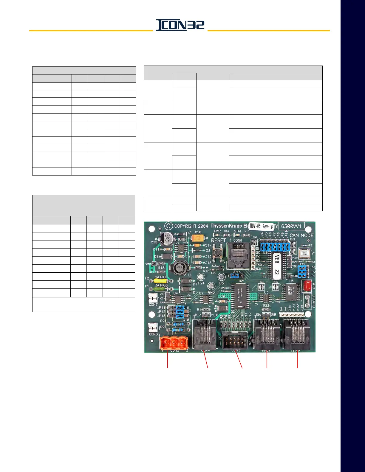
CAN Card Node (Channel 3)
Group Addressing
Note: This data not currently used.
JP3 JP2 JP1 JP8
CAR 1 OFF OFF OFF ON
CAR 2 OFF OFF ON ON
CAR 3 OFF ON OFF ON
CAR 4 OFFONONON
CAR 5 ON OFF OFF ON
CAR 6 ON OFF ON ON
CAR 7 ON ON OFF ON
CAR 8 ON ON ON ON
COMMON CAN*
OFF OFF OFF OFF
*These jumpers should remain OFF for
typical CAN applications.
CAN Auxiliary Jumper Settings
Jumper Position Default Description
JP9
ON
As
appropriate
Enables on-card port SPI I/O.
OFF
Disables on-card port SPI I/O.
Off-card SPI I/O only.
JP10 1 to 2
Not
Jumped
Provisional programming jumper.
JP11
and JP15
1 to 2
Not
Jumped
Connects the CAN communication shield
wiring to digital ground reference.
2 to 3
Connects the CAN communication shield
wiring to chassis ground reference.
JP12
1 to 2
Not
Jumped
Connects the CAN communication shield
wiring bypassing split capacitor.
2 to 3
Connects the CAN communication shield
wiring to split capacitor.
JP13
1 to 2
Not
Jumped
Connects the CAN communication split
capacitor to digital ground reference.
2 to 3
Connects the CAN communication split
capacitor to chassis ground reference.
JP14
1 to 2
1 to 2
Normal operation.
2 to 3 Programming uploading software.
CAN Card Node Addressing
JP7 JP6 JP5 JP4
CAN Card 0 OFF OFF OFF OFF
CAN Card 1 OFF OFF OFF ON
CAN Card 2 OFF OFF ON OFF
CAN Card 3 OFF OFF ON ON
CAN Card 4 OFF ON OFF OFF
CAN Card 5 OFF ON OFF ON
CAN Card 6 OFFONONOFF
CAN Card 7 OFFONONON
CAN Card 8 ON OFF OFF OFF
CAN Card 9 ON OFF OFF ON
CAN Card 10 ON OFF ON OFF
CAN Card 11 ON OFF ON ON