System Interface9
9 – 2
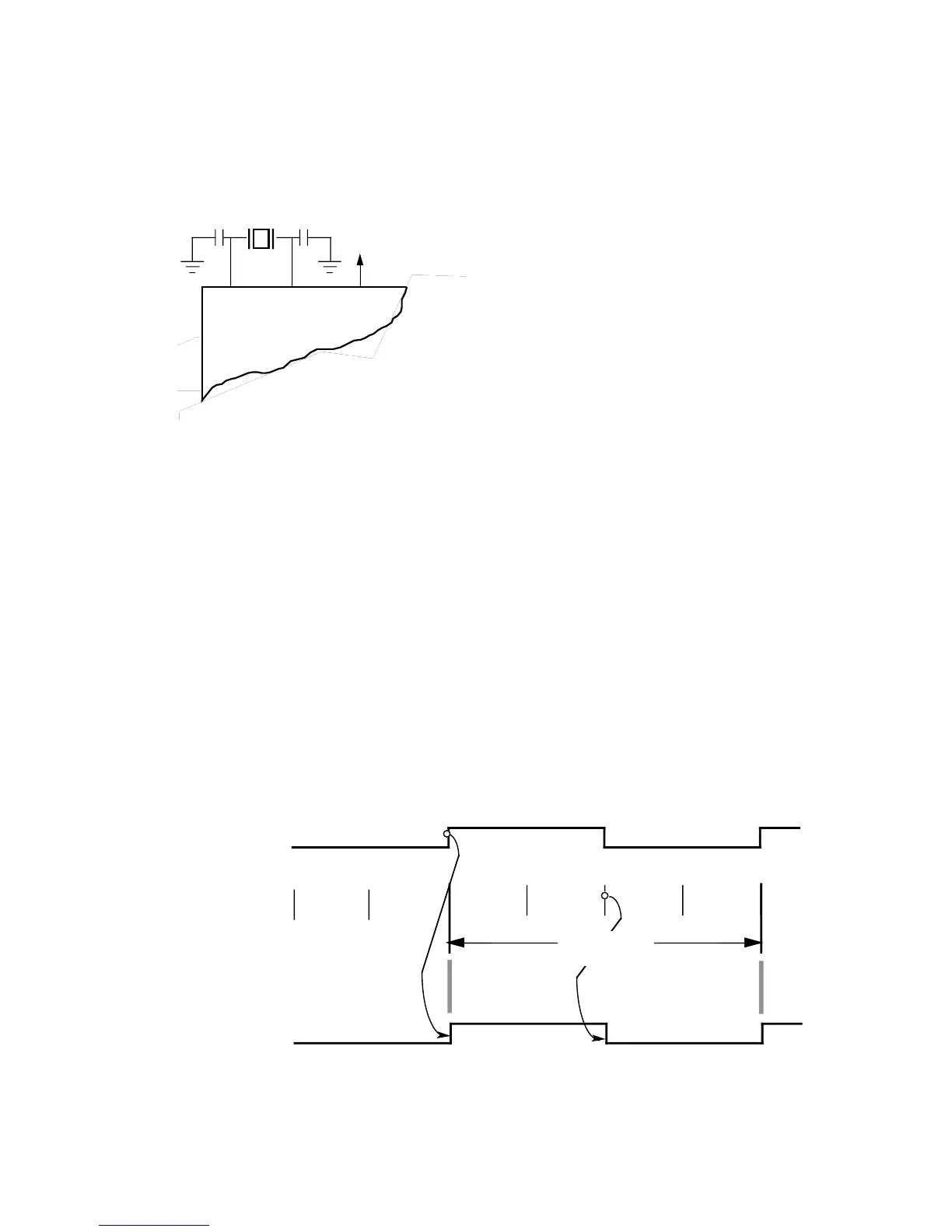
CLKIN CLKOUT
XTAL
Figure 9.1 External Crystal Connections
The internal phased lock loop of the processors generates an internal
clock which is four times the instruction rate.
The processors also generate a CLKOUT signal which is synchronized to
the processors’ internal cycles and operates at the instruction cycle rate. A
phase-locked loop is used to generate CLKOUT and to divide each
instruction cycle into a sequence of internal time periods called processor
states. The relationship between the phases of CLKIN, CLKOUT, and the
processor states is shown in Figure 9.2 for the ADSP-2101, ADSP-2105,
ADSP-2115, and ADSP-2111 processors. Figure 9.3 shows the same
information for the ADSP-2171, ADSP-2181, and ADSP-21msp58/59
processors. The phases of the internal processor clock are dependent upon
the period of the external clock.
The CLKOUT output can be disabled on the ADSP-2171, ADSP-2181, and
ADSP-21msp58/59 processors. This is controlled by the CLKODIS bit in
the SPORT0 Autobuffer Control Register.
ADSP-21xx
Figure 9.2 Clock Signals & Processor States (ADSP-2101, ADSP-2105, ADSP-2115, ADSP-
2111)
CLKIN
CLKOUT
INTERNAL
PROCESSOR
STATE
12 34
3 4
PROCESSOR
CYCLE

 Loading...

