System Interface9
9 – 16
(counter expired), the counter is not decremented as in other IF CE
instructions.
Flag outputs FL0, FL1 and FL2 are set to 1 at RESET. The Flag Out (F0) is
not affected by
RESET.
The ADSP-2181 has eight additional general-purpose flag pins, PF7-0.
These flags can be programmed as either inputs or outputs; they default to
inputs following reset. The PFx pins are programmed with the use of two
memory-mapped registers. The Programmable Flag & Composite Select
Control Register determines the flag direction: 1=output and 0=input. The
Programmable Flag Data Register is used to read and write the values on
the pins. Data being read from a pin configured as an input is
synchronized to the processor’s clock. Pins configured as outputs drive
the appropriate output value. When the PFDATA register is read, any
pins configured as outputs will read back the value being driven out.
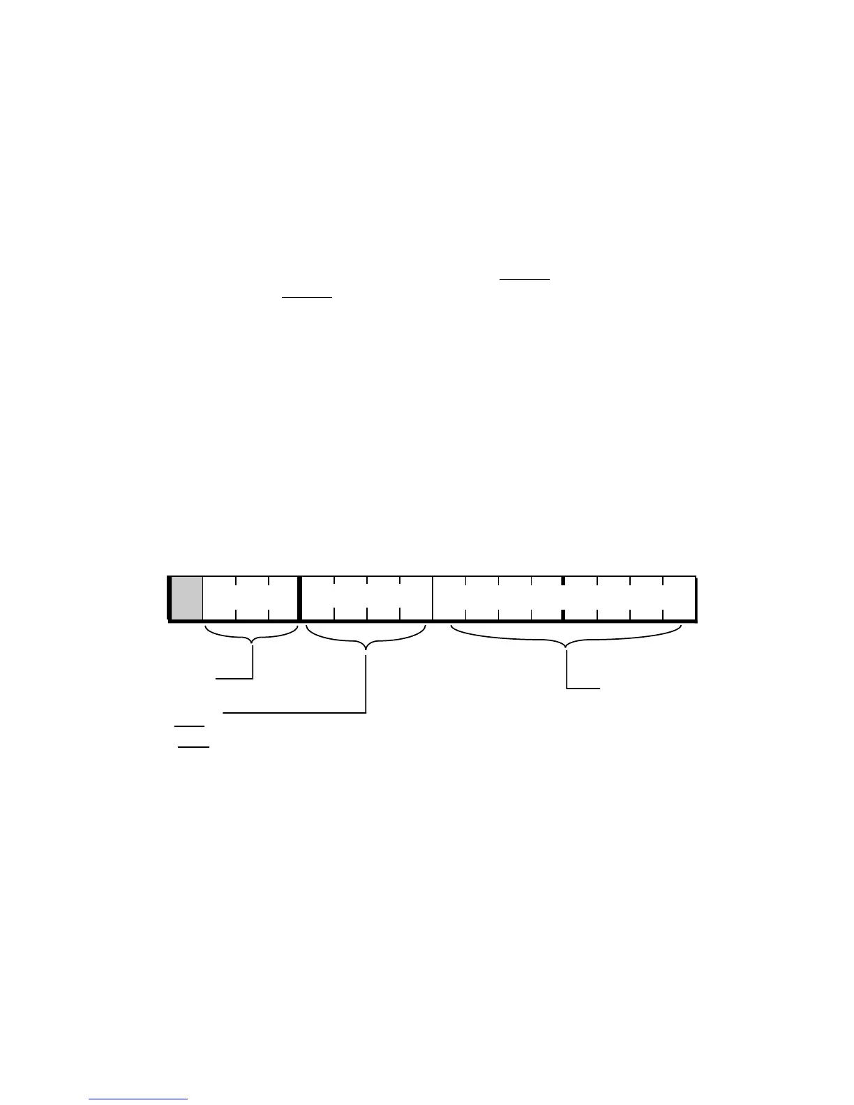
15 14 13 12 11 10 9 8 7 6 5 4 3 2 1 0
BMWAIT
1011110
Programmable Flag & Composite Select Control
PFTYPE
1 = Output
0 = Input
10000
CMSSEL
DM(0x3FE6)
0000
DMBMIOM PM
1 = Enable CMS
0 = Disable CMS
Figure 9.4 Programmable Flag & Composite Select Control Register (ADSP-
2181)

 Loading...

