10 Memory Interface
10 – 2
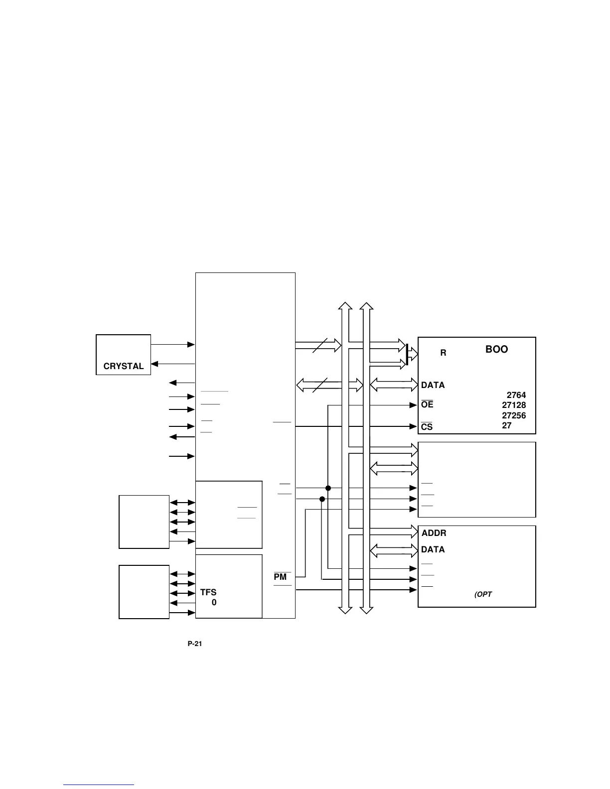
This chapter includes example timing diagrams for the memory interfaces
of the ADSP-21xx processors. For each bus transaction, only the sequence
of events is described; you must consult the processor data sheets for
actual timing parameters. All timing diagrams use CLKOUT as a
reference, which indicates the instruction execution rate.
The memory interfaces of the ADSP-2181 are described separately in the
second half this chapter.
BR
BG
CLKIN
RESET
IRQ2
BMS
ADSP-21xx
CLKOUT
AA
ADDR
DATA
(OPTIONAL)
A
1x CLOCK
or
CRYSTAL
PMS
DMS
RD
WR
ADDR
13-0
DATA
23-0
AA
AA
ADDR
DATA
(OPTIONAL)
AA
AA
ADDR
DATA
CS
OE
BOOT
MEMORY
e.g. EPROM
2764
27128
27256
27512
PROGRAM
MEMORY
DATA
MEMORY
&
PERIPHERALS
14
24
D
23-22
A
13-0
D
15-8
D
23-0
D
23-8
A
13-0
A
13-0
XTAL
MMAP
DR1
or
FI
SERIAL
DEVICE
(OPTIONAL)
DT1
or
FO
SCLK1
SPORT 1
DR0
DT0
TFS0
SCLK0
RFS0
SPORT 0
OE
WE
CS
RFS1
or
IRQ0
TFS1
or
IRQ1
SERIAL
DEVICE
(OPTIONAL)
OE
WE
CS
NOTES
1. Applies to all ADSP-21xx processors except ADSP-2181.
2. ADSP-2171 and ADSP-21msp58/59 use a 1/2x CLKIN signal.
3. Unused data bus lines may be left floating.
4. The two MSBs of the data bus (D23-22) are used to supply the two MSBs of the
boot memory EPROM address. This is only required for the 27256 and 27512.
Figure 10.1 ADSP-21xx System With External Memory

 Loading...

