Computational Units
2 – 23
2
MUX
16
32
SR1
REGISTER
SR0
REGISTER
16
SI
REGISTER
SB
REGISTER
MUX
MUX
SE
REGISTER
NEGATE
MUX
COMPARE
EXPONENT
DETECTOR
HI / LO
SHIFTER
ARRAY
IX
R
C
X
O
OR / PASS
MUXMUX
8
32
16
1616
From
INSTRUCTION
16
8
MUX
SS
DMD BUS
R - BUS
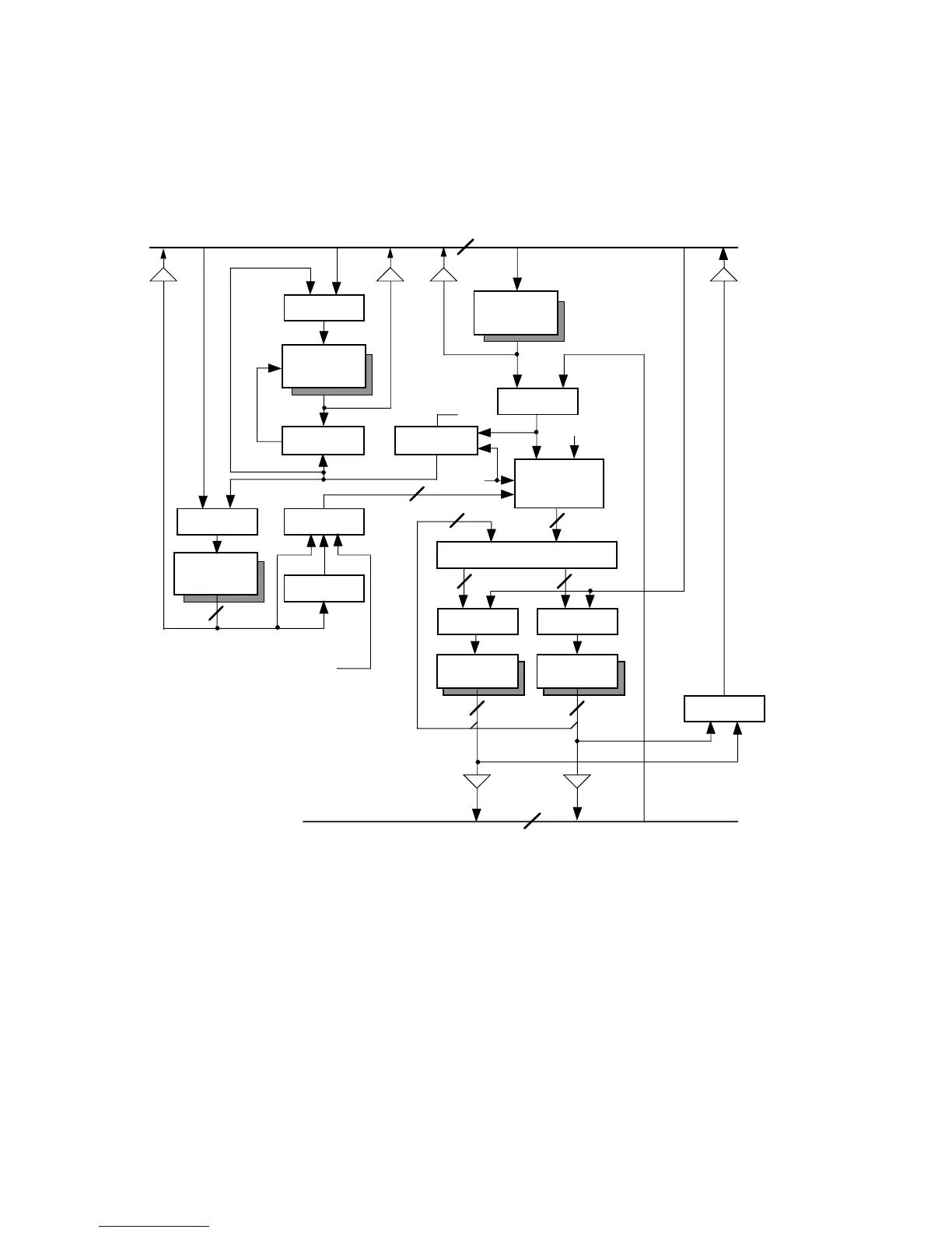
Figure 2.9 Shifter Block Diagram
Any of the SI, SE or SR registers can be read and written in the same cycle.
Registers are read at the beginning of the cycle and written at the end of
the cycle. All register reads, therefore, read values loaded at the end of a
previous cycle. A new value written to a register cannot be read out until a
subsequent cycle. This allows an input register to provide an operand to
the shifter at the beginning of the cycle and be updated with the next
operand at the end of the same cycle. It also allows a result register to be
stored in memory and updated with a new result in the same cycle. See
the discussion of “Multifunction Instructions” in Chapter 15, “Instruction
Set Reference” for an illustration of this same-cycle read and write.
 Loading...


