GR740-UM-DS, Nov 2017, Version 1.7 443 www.cobham.com/gaisler
GR740
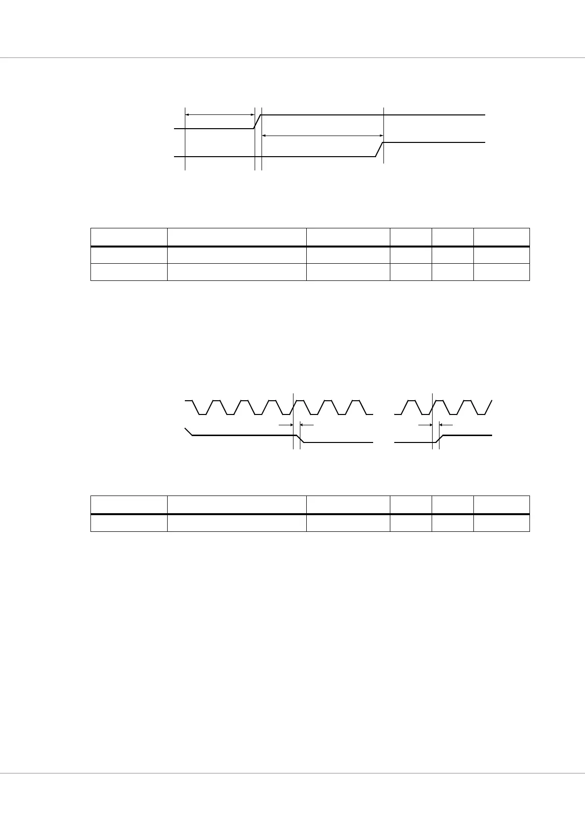
39.5.3 Phase-locked loop timings
The timing waveforms and timing parameters are shown in figure 56 and are defined in table 580.
39.5.4 Processor error mode signal timing
The timing waveforms and timing parameters are shown in figure 57 and are defined in table 581.
Table 580.Timing parameters
Name Parameter Reference edge Min Max Unit
t
PLL0
PLL power-down duration
1)
-
10000
2)
-
ns
t
PLL1
PLL locking time
rising sys_resetn
- 100000 ns
Notes:
1)
PLL is in power-down as long as sys_resetn is held low. Unused PLLs for selected configuration are permanently in
power-down and their corresponding lock signals never go high.
2)
This parameter is not tested.
Table 581.Timing parameters
Name Parameter Reference edge Min Max Unit
t
LEON4_0
clock to output tri-state delay rising clk edge
0
1)
30
2)
ns
Notes:
1)
This parameter is guaranteed by design and is not tested
2)
This parameter is determined by static timing analysis and is not tested
Figure 56. Timing waveforms
pll_locked[5:0]
sys_resetn
t
PLL0
t
PLL1
Figure 57. Timing waveforms
t
LEON4_0
proc_errorn
internal clk
t
LEON4_0