GR740-UM-DS, Nov 2017, Version 1.7 445 www.cobham.com/gaisler
GR740
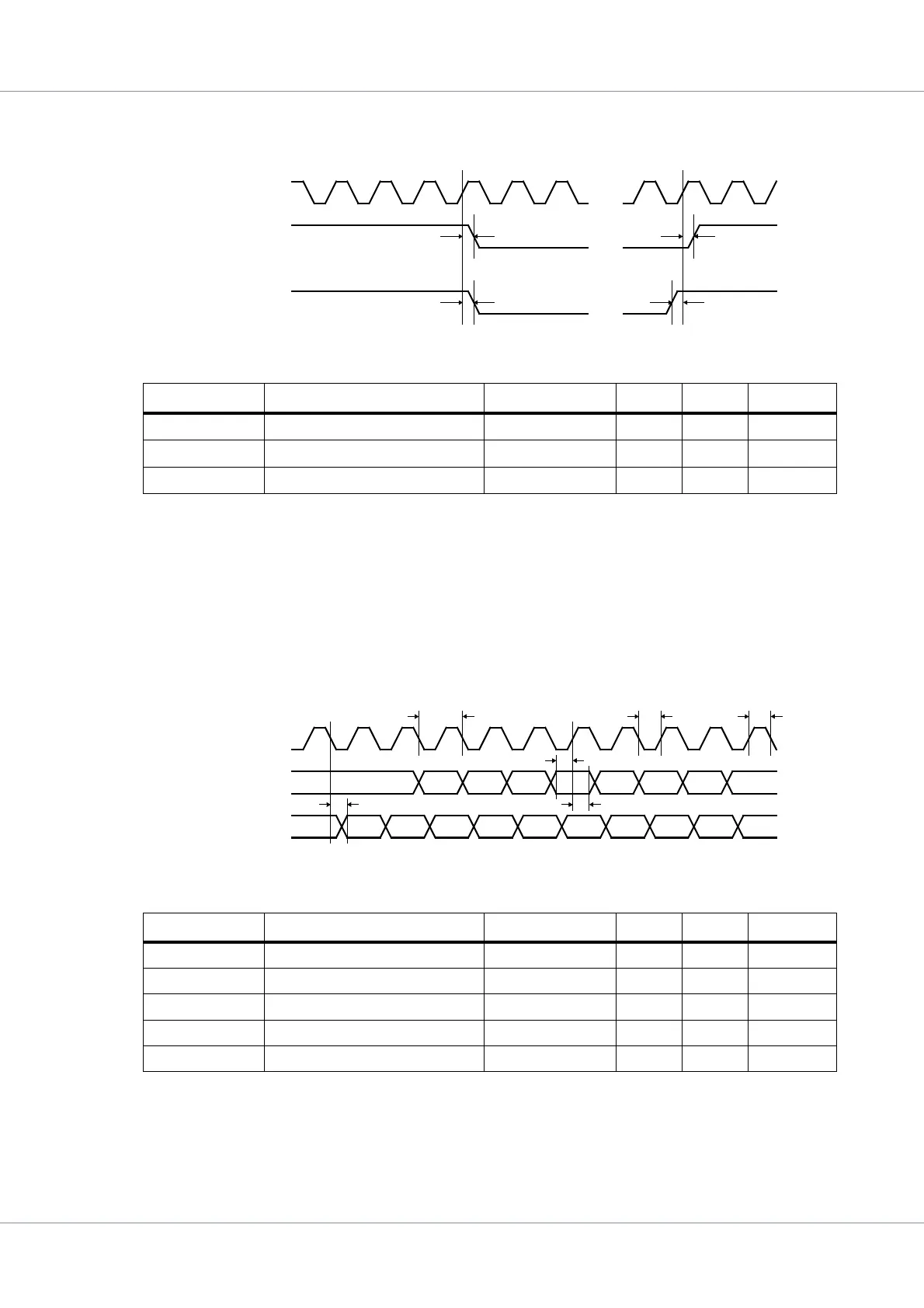
39.5.6 DSU signals timing
The timing waveforms and timing parameters are shown in figure 59 and are defined in table 583.
39.5.7 JTAG interface timing
The timing waveforms and timing parameters are shown in figure 60 and are defined in table 584.
Table 583.Timing parameters
Name Parameter Reference edge Min Max Unit
t
DSU0
clock to output delay rising clk edge
0
1)
30
2)
ns
t
DSU1
input to clock hold rising clk edge
-
3)
-
3)
ns
t
DSU2
input to clock setup rising clk edge
-
3)
-
3)
ns
Notes:
1)
This parameter is guaranteed by design and is not tested
2)
This parameter is determined by static timing analysis and is not tested
3)
The break and dsu_en signals are re-synchronized internally. These signals do not have to meet any setup or hold
requirements. As the dsu_en signal controls clock gating for the Debug AHB bus the signal’s value should be kept con-
stant from power-up.
Table 584.Timing parameters
Name Parameter Reference edge Min Max Unit
t
AHBJTAG0
clock period - 45 - ns
t
AHBJTAG1
clock low/high period - 20 - ns
t
AHBJTAG2
data input to clock setup rising jtag_tck edge 20 - ns
t
AHBJTAG3
data input from clock hold rising jtag_tck edge 20 - ns
t
AHBJTAG4
clock to data output delay falling jtag_tck edge 0 15 ns
Figure 59. Timing waveforms
t
DSU0
dsu_active
internal clk
t
DSU0
t
DSU1
dsu_en, break t
DSU2
Figure 60. Timing waveforms
jtag_tdi, jtag_tms
jtag_tck
jtag_tdo
t
AHBJTAG3
t
AHBJTAG4
t
AHBJTAG2
t
AHBJTAG0
t
AHBJTAG1