GR740-UM-DS, Nov 2017, Version 1.7 454 www.cobham.com/gaisler
GR740
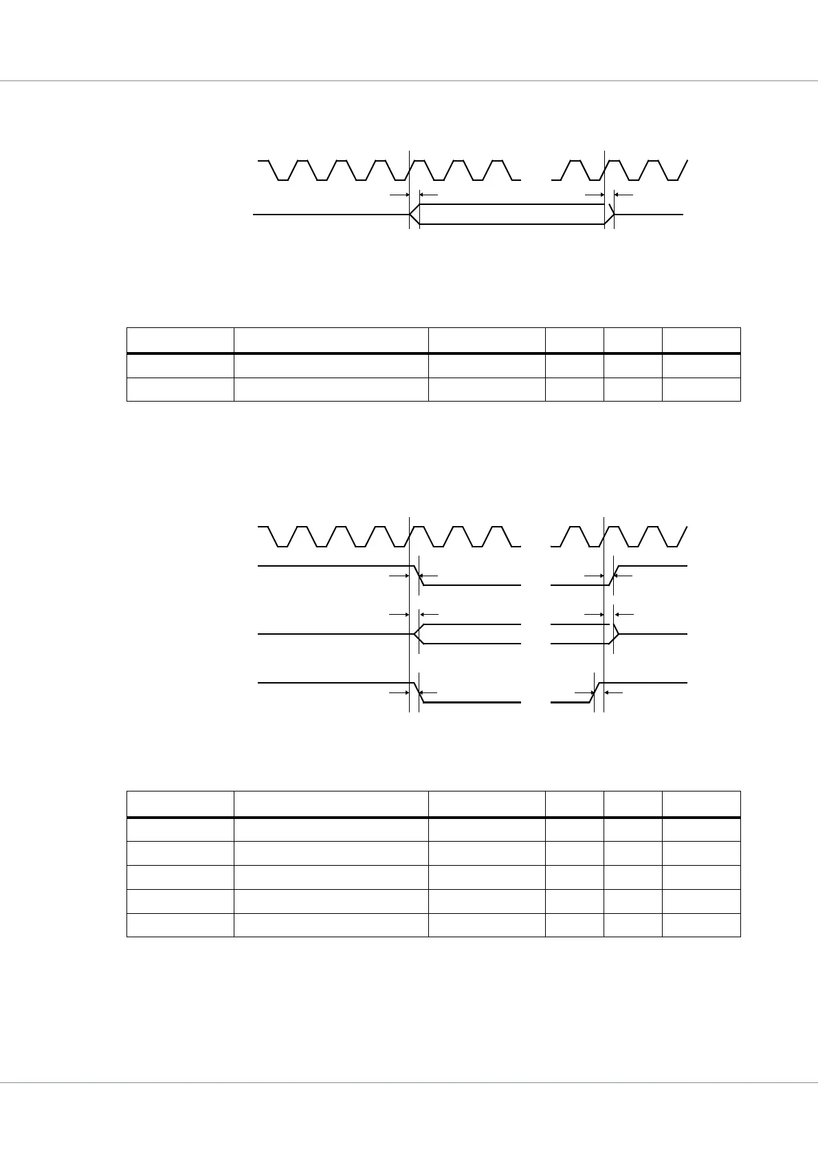
39.5.15 Watchdog signal timing
The timing waveforms and timing parameters are shown in figure 69 and are defined in table 592.
39.5.16 General Purpose I/O interface timing
The timing waveforms and timing parameters are shown in figure 70 and are defined in table 593.
Table 592.Timing parameters
Name Parameter Reference edge Min Max Unit
t
GPTIMER0
clock to output tri-state rising clk edge
0
1)
40
2)
ns
t
GPTIMER1
clock to output delay rising clk edge
0
1)
40
2)
ns
1) Guaranteed by design, not tested
2) Verified by static timing analysis, not tested
Table 593.Timing parameters
Name Parameter Reference edge Min Max Unit
t
GRGPIO0
clock to output delay rising clk edge
0
1)
40
2)
ns
t
GRGPIO1
clock to non-tri-state delay rising clk edge
0
1)
40
2)
ns
t
GRGPIO2
clock to tri-state delay rising clk edge
0
1)
40
2)
ns
t
GRGPIO3
input to clock hold
rising clk edge
3)
--ns
t
GRGPIO4
input to clock setup
rising clk edge
3)
--ns
1)
Guaranteed by design, not tested.
2)
Verified by static timing analysis, not tested
3)
The gpio inputs are re-synchronized internally. The signals do not have to meet any setup or hold requirements.
Figure 69. Timing waveforms
t
GPTIMER0
wdogn
internal sys_clk
t
GPTIMER1
Figure 70. Timing waveforms
t
GRGPIO0
gpio[ ]
internal sys_clk
t
GRGPIO0
t
GRGPIO1
gpio[ ]
t
GRGPIO2
t
GRGPIO3
gpio[ ] t
GRGPIO4
(output)
(output)
(input)