GR740-UM-DS, Nov 2017, Version 1.7 456 www.cobham.com/gaisler
GR740
39.5.18 SPI controller timing
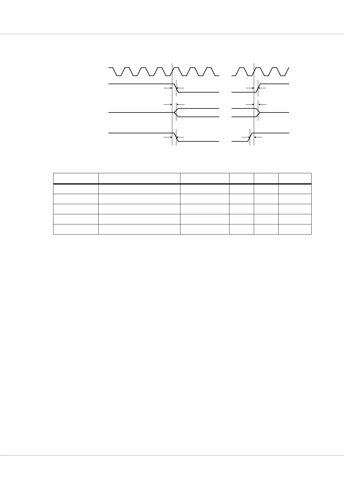
The timing waveforms and timing parameters are shown in figure 72 and are defined in table 595.
Table 595.Timing parameters
Name Parameter Reference edge Min Max Unit
t
SPICTRL0
clock to output delay rising clk edge
0
1)
40
2)
ns
t
SPICTRL1
clock to non-tri-state delay rising clk edge
0
1)
40
2)
ns
t
SPICTRL2
clock to tri-state delay rising clk edge
0
1)
40
2)
ns
t
SPICTRL3
input to clock hold
rising clk edge
3)
--ns
t
SPICTRL4
input to clock setup
rising clk edge
3)
--ns
1)
Guaranteed by design, not tested.
2)
Verified by static timing analysis, not tested
3)
The spi_sck/miso/mosi/spisel inputs are re-synchronized internally. The signals do not have to meet any setup or hold
requirements. However, the input to clock setup value restricts the maximum SPI frequency.
Figure 72. Timing waveforms
t
SPICTRL0
spi_sck/miso/mosi/slvsel
internal sys_clk
t
SPCTRLI0
t
SPICTRL1
spi_sck/miso/mosi
t
SPICTRL2
t
SPICTRL3
spi_sck/miso/mosi/sel t
SPICTRL4
(output)
(output)
(input)