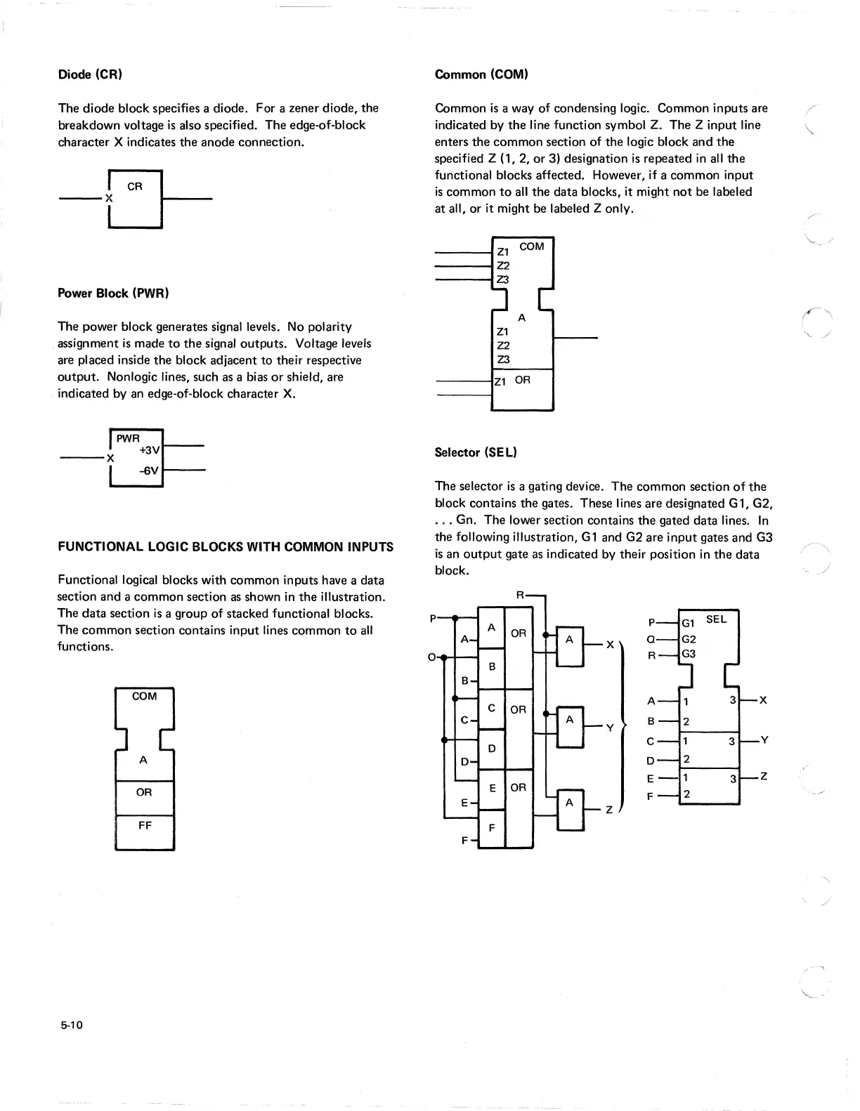
Diode (CR)
The diode block specifies a diode. For a zener diode, the
breakdown voltage
is
also specified. The edge-of-block
character X indicates
the
anode connection.
~
---u-
Power
Block
(PWR)
The power block generates signal levels. No polarity
assignment
is
made
to
the
signal outputs. Voltage levels
are placed inside
the
block adjacent
to
their respective
output.
Nonlogic lines, such
as
a bias
or
shield, are
indicated by
an
edge-of-block character
X.
---~
L:T-
FUNCTIONAL LOGIC BLOCKS WITH
COMMON
INPUTS
Functional logical blocks with common inputs have a data
section and a common section
as
shown
in
the
illustration.
The data section
is
a group of stacked functional blocks.
The common section contains input lines common
to
all
functions.
COM
A
OR
FF
5-10
Common
(COM)
Common
is
a way of condensing logic. Common inputs are
indicated by
the
line function symbol Z. The Z input line
enters
the
common section of the logic block and
the
specified Z (1, 2,
or
3) designation
is
repeated
in
all
the
functional blocks affected. However, if a common input
is
common
to
all
the
data blocks, it might
not
be labeled
at all, or it might be labeled Z only.
----4Z1
COM
----121
----4Z3
Z1
Z2
Z3
A
----fZ1
OR
Selector
(SE
L)
The selector
is
a gating device. The common section
of
the
block contains the gates. These lines are designated G1, G2,
...
Gn. The lower section contains the gated data lines.
In
the following illustration,
G1
and G2 are input gates and G3
is
an
output
gate
as
indicated by their position
in
the
data
block.
p
p
SEL
A
X
Q
0
R
A
3 X
OR
A
B
Y
C 3
y
0
E
3
Z
F
2
Z
F
F
/
'\
{
'-
. ..-"