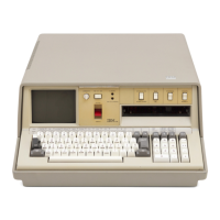
5100 CONTROLLER DESCRIPTION
The Controller
Data
Flow diagram shows the organization
of
the controller.
The 5100 controller card
(G2)
controls the data
flow
throughout the computing system. The controller
communicates with executable
ROS,
base
I/O,
read/write
storage, and the display adapter. Control
pulses and clock pulses are also generated on the
controller card.
Storage
Read
Bus
and
Storage
Write
Bus
The storage read bus and the storage write bus are
18-bit
buses.
Each
is used
to
transfer 2 bytes
of
data
having even parity. The storage read bus and the
storage write bus are used during the following
operations:
• Reading from executable
ROS
• Reading from
read/write
storage
• Writing into
read/write
storage
• Sending information from
read/write
storage
to
the display unit
Da,ta Bus
In
The data bus
in
is a
9-bit
bus used
to
transfer 1 byte
of
data plus parity from the base
I/O
card
to
the
controller.
Data
Bus
Out
The data bus out is a
9-bit
bus used
to
transfer 1 byte
of
data plus parity from the controller
to
the base
I/O
card.
Storage
Address
Bus
The storage address bus is a
16-bit
bus used
to
supply
addresses
to
read/write
storage or executable
ROS.
The display adapter sends storage addresses
to
the
processor via the storage address bus by cycle steal
transfers.
4·16
Internal
Controller
Organization
(Refer
to
the
5100
Controller Data Flow diagram.)
Read
Data Registers: The
RDR
registers receive
two
bytes
of
data on each storage read operation via the
storage read bus.
From the read data register, operands
can
be transferred
to
the storage address register (SAR), the operations
register (Op
Reg).
the storage data register (SDR). or the
arithmetic logic unit register (ALU
Reg).
Storage Address Register (SAR): The storage address
register is a
16-bit
register used
to
address storage.
Operation Register (Op Reg): The operation register is a
16-bit
register used
to
decode the op code.
Storage Data Register (SDR): The storage data register
is
an
8-bit
(1-byte) register used
to
receive data
through the data bus in. The register also provides the
second operand input
to
the ALU.
Arithmetic
and
Logic Unit Register
(AW
Reg): The
arithmetic and logic unit register is
an
8-bit
register that
receives
1-byte
operands from the read data register.
The output
of
the ALU register provides the first
operand input
to
ALU and also provides data
for
the
data bus out.
Arithmetic
and
Logic Unit Register (ALU): The arithmetic
and logic unit is
an
8-bit
(1-byte) binary unit. When
two
8-bit
operands are presented
to
its inputs, the ALU
produces
an
8-bit
arithmetic or logical result at its
output.
Control
ROS
Unit: The control
ROS
unit generates the
necessary control lines and gating signals
for
the
instruction being executed.
Registers: The registers on the controller card are
addressed
as
the first 128 bytes
of
read/write
storage
and
are associated with the four interrupt levels in which
processing occurs.
,/