(
(
(
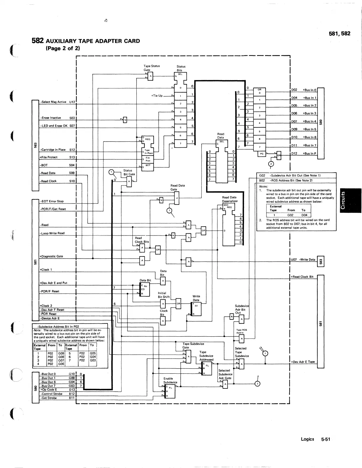
582 AUXILIARY TAPE ADAPTER CARD
(Page 2
of
2)
r-------------
------------------,
I
I
TGaatePe
Status Status
II
Bits
I
-.t{j"
G SEL
I
I 0
r--2-
I +Tie
Up
------"
--;--
r-l
!002
+Bus InO
r--
r--
-select
Mag
Active
U121 - 2
2
t----"
..,
18
I
----'>
--;-
r-2
-Erase Inactive 503 i - 4
~~~~~--~~----_+_+--------~N~--~------+_--~~
4
~
-
-LED and Erase
OK
507 i
~~~~==~~~------+_~--------------~------~----~
5
r-2
1
I
512
1
-Cartridge in Place
+File
Protect
513:
.------+~~
~~~~~==~~~------~+_+_------------_t_1s~~.~~
~~~~~--~~~------r_+_+_------------_+_;~I___
r Prol
-
---"
6
~
-
r'" 7
r-2-
--
-BOT
504\
r-;;;:-
~~--------~~~------r_+_+_------------_+~s
r------
-Read Data 509
-Read
Cloci<
5101
~te
'--
~
!004
+Bus
In
1
!OOS
+8U5
In
2
006
+Bus
In
3
!007
+Bus
In
4
Ii!
!009
"'
+Bus
In
5
2_
-:0-
2
3 L
--;-1--
______ --+='---'-"==_1
4
..L
--:-1----------+='---'-"==-1
1
010
+Bus
In
6
011
+Bus
In
7
0
012
+Bus
In
P
-
2
I
G02
-Subdevice
Adr
Bit
Out
(See
Note
1)
B02
-ROS Address Bit
(5
..
Note
2)
r Notes:
581,582
'--
I
I
r-
-EOT
Error Stop
I
Read
Data
Gate
Read
Data
~
Deserializer
SOD
1.
The
subdevice
adr
bit
out
pin will
be
externally
wired
to
a bus in pin
on
the
pin side
of
the
card
socket. Each additional
tape
will have a
uniquely
wired subdevice address as shown below:
-POR/F/Get Reset
I
_ A REG
I
-Read
I
L-+-------I---t-----------t-----------~~A
-Loop
Write Read
."
N
ORr--r_t--t
D
Read
--?,
~
---E.
-4
~
-?-
2.
External
Tape
L 1
From
G02
To
J
004
The
AOS address
bit
will
be
wired on
the
card
socket
trom
802
to
007;
bus
in
bit
4,
for
all
additional external
tape
units.
I
I
L-
__
-r
______
-I
__
-+
_____
~-C~IO~C:Bits
--b
--..2.
-
OR~+_-----+------------~_+
+Diagnostic Gate
:;;
1
"'
-+Clock
1
+Oev
Adr
E
and
Put
!
-POR/F Reset
i
I
-+Clock
2
I
-Dev
Adr
F Reset
I
-POR Reset
-Oevice
Adr
E
~Subdevice
Address Bit In
P02
Note:
The
subdevice address
bit
in pin
will
be
ex·
ternally wired
to
a bus
out
pin
on
the
pin side
of
the
card socket. Each additional tape
unit
will have
a
uniquely
wired subdevice address as shown below:
External
From
To
Extemal
From
To
!
Tape Tape
1
P02
GOO
5
2
P02
GOB
6
3 P02 G07 7
4 P02 G06
P02
P02
P02
G05
G04
GOO
7
6
II'
A
~--;
--w
'----+-i
Data
Bit
Data
Bit
A
t;j
CD
..I
R
Initial
Bit
Shift
Write
Data
A
OR
fj
Cloci<
Bit
A
Subdevice
AdrBit
~
I U07 -Write
Data
C"J
!l!
i
I+Read Clock Bit
r-
I
1
I
I
I
I
TapeAOS
I
~------------t_1----------------------------4--_1-A-·~rd~l"
R.:J-
I
l;[hf
t
~!""
~
I
'-I---_t------------_t_1----------~
A Subdevice Subdevice I
r-1-_t--------~"'t
Adt
essed
-.rJ
A I +Oev Adr E Tape
...
FL ,
~I·I
I
+--------+-------"tJ~
Selected
~
r--
=:~:
~~: ~
~~
I
~
i Enable A
.!!-.
~~~;.:~e
I
!
~~~~!!!~!.:
g=~~ui'-:e~:-E----.....,,~:=r~;t-"~-I
: J j:1
.:.'
II
-Control 51robe B 12
-Get5trobe
Bll
....
________________
~
________________
J
Logics
5-51
 Loading...