System Integration Module (SIM)
Technical Data MC68HC908AB32 — Rev. 1.0
112 System Integration Module (SIM) MOTOROLA
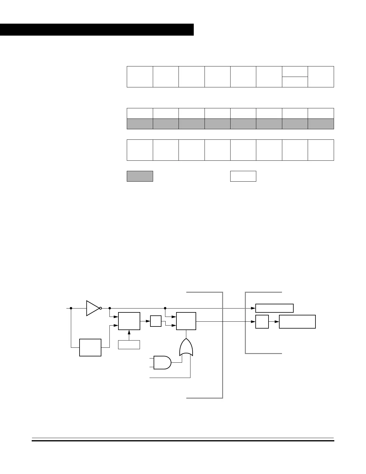
8.3 SIM Bus Clock Control and Generation
The bus clock generator provides system clock signals for the CPU and
peripherals on the MCU. The system clocks are generated from an
incoming clock, CGMOUT, as shown in Figure 8-3. This clock can come
from either an external oscillator or from the on-chip PLL.
See Section 9. Clock Generator Module (CGM).
Figure 8-3. CGM Clock Signals
Addr. Register Name Bit 7 654321Bit 0
$FE00
SIM Break Status Register
(SBSR)
Read:
RRRRRR
SBSW
R
Write: Note
Reset: 00000000
Note: Writing a logic 0 clears SBSW.
$FE01
SIM Reset Status Register
(SRSR)
Read: POR PIN COP ILOP ILAD 0 LVI 0
Write:
POR: 10000000
$FE03
SIM Break Flag Control
Register
(SBFCR)
Read:
BCFE RRRRRRR
Write:
Reset: 0
= Unimplemented
R
= Reserved
Figure 8-2. SIM I/O Register Summary
PLL
OSC1
CGMXCLK
÷ 2
BUS CLOCK
GENERATORS
SIM
CGM
SIM COUNTER
MONITOR MODE
CLOCK
SELECT
CIRCUIT
CGMVCLK
BCS
÷ 2
A
B
S
*
CGMOUT
*When S = 1,
CGMOUT = B
USER MODE
PTC3
 Loading...


