Clock Generator Module (CGM)
Functional Description
MC68HC908AB32 — Rev. 1.0 Technical Data
MOTOROLA Clock Generator Module (CGM) 141
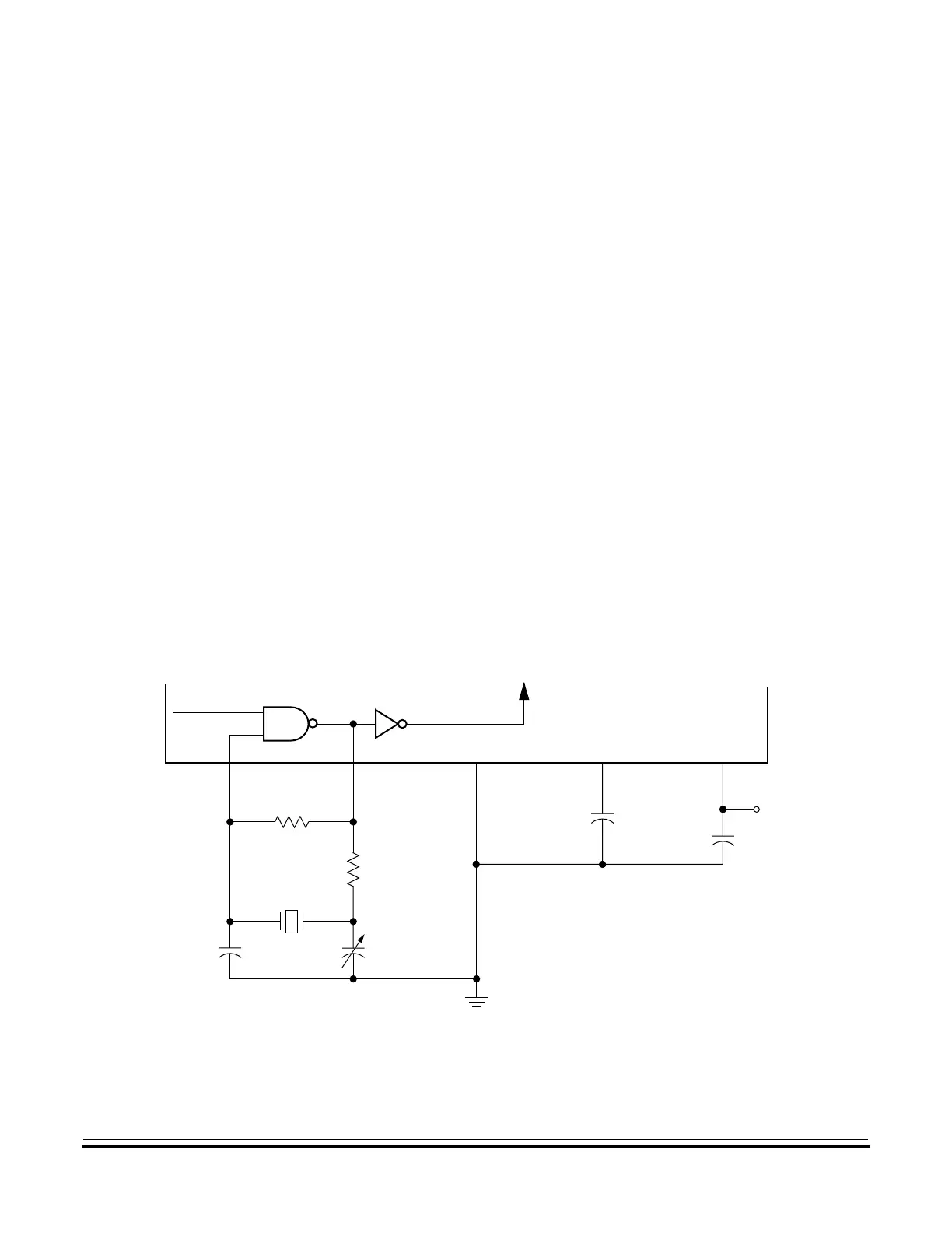
• Crystal, X
1
• Fixed capacitor, C
1
• Tuning capacitor, C
2
(can also be a fixed capacitor)
• Feedback resistor, R
B
• Series resistor, R
S
(optional)
The series resistor (R
S
) is included in the diagram to follow strict Pierce
oscillator guidelines and may not be required for all ranges of operation,
especially with high frequency crystals. Refer to the crystal
manufacturer’s data for more information.
Figure 9-3 also shows the external components for the PLL:
• Bypass capacitor, C
BYP
• Filter capacitor, C
F
Care should be taken with routing in order to minimize signal cross talk
and noise. (See 9.10 Acquisition/Lock Time Specifications for routing
information and more information on the filter capacitor’s value and its
effects on PLL performance).
Figure 9-3. CGM External Connections
C
1
C
2
C
F
SIMOSCEN
CGMXCLK
R
B
X
1
R
S
*
C
BYP
*R
S
can be zero (shorted) when used with higher-frequency crystals. Refer to manufacturer’s data.
OSC1 OSC2 V
SSA
CGMXFC V
DDA
V
DD
 Loading...


