Input/Output (I/O) Ports
Technical Data MC68HC908AB32 — Rev. 1.0
322 Input/Output (I/O) Ports MOTOROLA
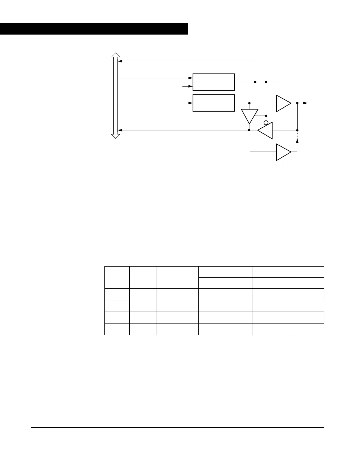
Figure 17-10. Port C I/O Circuit
When DDRCx is a logic 1, reading address $0002 reads the PTCx data
latch. When DDRCx is a logic 0, reading address $0002 reads the
voltage level on the pin. The data latch can always be written, regardless
of the state of its data direction bit.
Table 17-4 summarizes the operation of the port C pins.
Table 17-4. Port C Pin Functions
DDRC
Bit
PTC Bit I/O Pin Mode
Accesses to DDRC Accesses to PTC
Read/Write Read Write
0 2 Input, Hi-Z DDRC7 Pin PTC2
1 2 Output DDRC7 0 —
0X
(1)
Notes:
1. X = don’t care; except PTC2.
Input, Hi-Z
(2)
2. Hi-Z = high impedance.
DDRC[5:0] Pin PTC[5:0]
(3)
3. Writing affects data register, but does not affect input.
1 X Output DDRC[5:0] PTC[5:0] PTC[5:0]
READ DDRC ($0006)
WRITE DDRC ($0006)
RESET
WRITE PTC ($0002)
READ PTC ($0002)
PTCx
DDRCx
PTCx
INTERNAL DATA BUS
MCLK
MCLKEN
PTC2 ONLY
 Loading...


