Timer Interface Module A (TIMA)
Technical Data MC68HC908AB32 — Rev. 1.0
192 Timer Interface Module A (TIMA) MOTOROLA
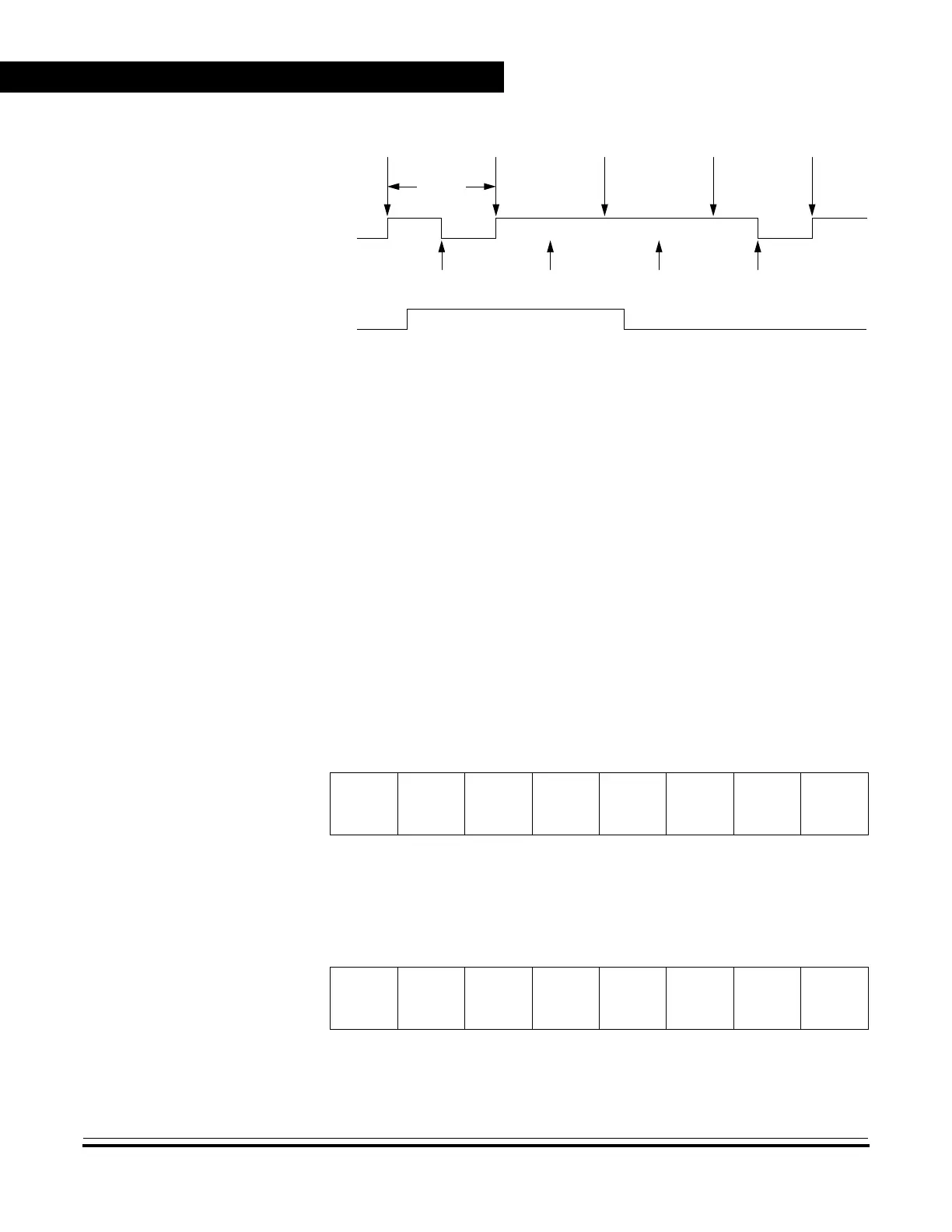
Figure 11-13. CHxMAX Latency
11.10.5 TIMA Channel Registers
These read/write registers contain the captured TIMA counter value of
the input capture function or the output compare value of the output
compare function. The state of the TIMA channel registers after reset is
unknown.
In input capture mode (MSxB:MSxA = 0:0), reading the high byte of the
TIMA channel x registers (TACHxH) inhibits input captures until the low
byte (TACHxL) is read.
In output compare mode (MSxB:MSxA ≠ 0:0), writing to the high byte of
the TIMA channel x registers (TACHxH) inhibits output compares until
the low byte (TACHxL) is written.
OUTPUT
OVERFLOW
TACHx
PERIOD
CHxMAX
OVERFLOW OVERFLOW OVERFLOW OVERFLOW
COMPARE
OUTPUT
COMPARE
OUTPUT
COMPARE
OUTPUT
COMPARE
Address: $0027
Bit 7 654321Bit 0
Read:
Bit 15 14 13 12 11 10 9 Bit 8
Write:
Reset: Indeterminate after reset
Figure 11-14. TIMA Channel 0 Register High (TACH0H)
Address: $0028
Bit 7 654321Bit 0
Read:
Bit 7 654321Bit 0
Write:
Reset: Indeterminate after reset
Figure 11-15. TIMA Channel 0 Register Low (TACH0L)
 Loading...


