FLASH Memory
FLASH Block Protection
MC68HC908AB32 — Rev. 1.0 Technical Data
MOTOROLA FLASH Memory 65
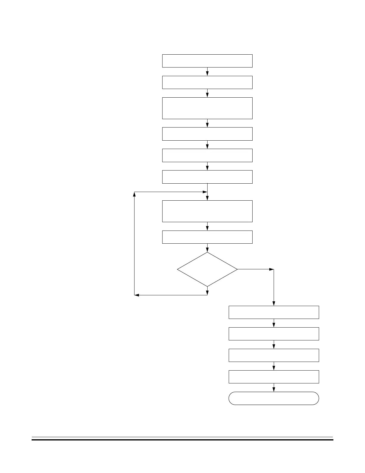
Figure 4-2. FLASH Programming Flowchart
Set HVEN bit
Read the FLASH block protect register
Write any data to any FLASH address
within the row address range desired
Wait for a time, t
nvs
Set PGM bit
Wait for a time, t
pgs
Write data to the FLASH address
to be programmed
Wait for a time, t
PROG
Clear PGM bit
Wait for a time, t
nvh
Clear HVEN bit
Wait for a time, t
rcv
Completed
programming
this row?
Y
N
End of programming
The time between each FLASH address change (step 7 to step 7), or
must not exceed the maximum programming
time, t
PROG
max.
the time between the last FLASH address programmed
to clearing PGM bit (step 7 to step 10)
NOTE:
1
2
3
4
5
6
7
8
10
11
12
13
Algorithm for programming
a row (64 bytes) of FLASH memory
This row program algorithm assumes the row/s
to be programmed are initially erased.
 Loading...


