General Description
Technical Data MC68HC908AB32 — Rev. 1.0
38 General Description MOTOROLA
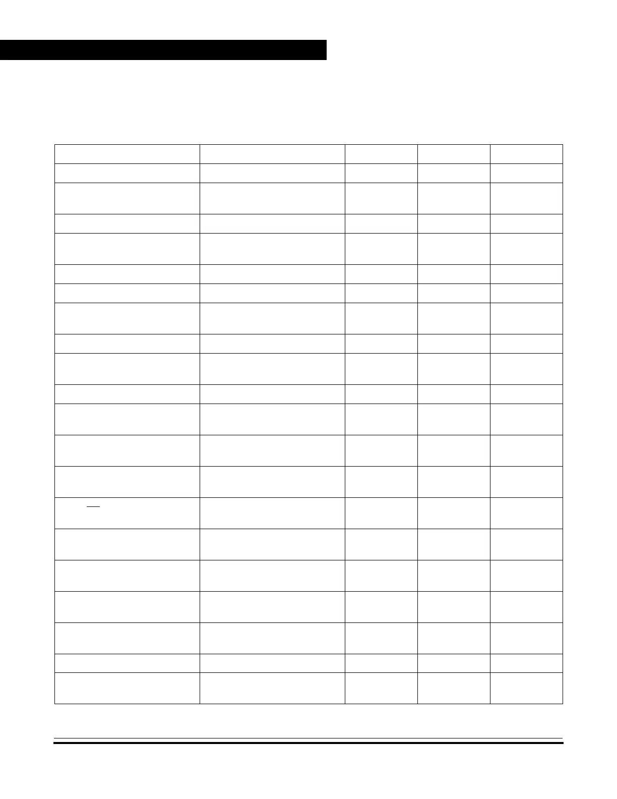
1.7 I/O Pin Summary
Table 1-1. I/O Pins Summary
Pin Name Function Driver Type Hysteresis Reset State
PTA7–PTA0 General purpose I/O Dual State No Input (Hi-Z)
PTB7/ATD7–PTB0/ATD0
General purpose I/O
/ ADC channel
Dual State No Input (Hi-Z)
PTC5–PTC3 General purpose I/O Dual State No Input (Hi-Z)
PTC2/MCLK
General purpose I/O
/ System clock
Dual State No Input (Hi-Z)
PTC1–PTC0 General purpose I/O Dual State No Input (Hi-Z)
PTD7 General purpose I/O Dual State No Input (Hi-Z)
PTD6/TACLK
General purpose I/O
/ Timer external input clock
Dual State No Input (Hi-Z)
PTD5 General purpose I/O Dual State No Input (Hi-Z)
PTD4/TBCLK
General purpose I/O
/ Timer external input clock
Dual State No Input (Hi-Z)
PTD3–PTD0 General purpose I/O Dual State No Input (Hi-Z)
PTE7/SPSCK
General purpose I/O
/ SPI clock
Dual State
(open drain)
Yes Input (Hi-Z)
PTE6/MOSI
General purpose I/O
/ SPI data path
Dual State
(open drain)
Yes Input (Hi-Z)
PTE5/MISO
General purpose I/O
/ SPI data path
Dual State
(open drain)
Yes Input (Hi-Z)
PTE4/SS
General purpose I/O
/ SPI slave select
Dual State Yes Input (Hi-Z)
PTE3/TACH1
General purpose I/O
/ Timer A channel 1
Dual State Yes Input (Hi-Z)
PTE2/TACH0
General purpose I/O
/ Timer A channel 0
Dual State Yes Input (Hi-Z)
PTE1/RxD
General purpose I/O
/ SCI receive data
Dual State Yes Input (Hi-Z)
PTE0/TxD
General purpose I/O
/ SCI transmit data
Dual State Yes Input (Hi-Z)
PTF7–PTF6 General purpose I/O Dual State Yes Input (Hi-Z)
PTF5/TBCH1
General purpose I/O
/ Timer B channel 1
Dual State Yes Input (Hi-Z)
 Loading...


