Clock Generator Module (CGM)
Technical Data MC68HC908AB32 — Rev. 1.0
146 Clock Generator Module (CGM) MOTOROLA
the other. During the transition, CGMOUT is held in stasis. See 9.4.3
Base Clock Selector Circuit. Reset and the STOP instruction clear
the BCS bit.
1 = CGMOUT driven by CGMVCLK/2
0 = CGMOUT driven by CGMXCLK/2
NOTE:
PLLON and BCS have built-in protection that prevents the base clock
selector circuit from selecting the VCO clock as the source of the base
clock if the PLL is off. Therefore, PLLON cannot be cleared when BCS
is set, and BCS cannot be set when PLLON is clear. If the PLL is off
(PLLON = 0), selecting CGMVCLK requires two writes to the PLL control
register. See 9.4.3 Base Clock Selector Circuit.
Bits [3:0] — Unimplemented bits
These bits provide no function and always read as 1.
9.6.2 PLL Bandwidth Control Register (PBWC)
The PLL bandwidth control register does the following:
• Selects automatic or manual (software-controlled) bandwidth
control mode
• Indicates when the PLL is locked
• In automatic bandwidth control mode, indicates when the PLL is in
acquisition or tracking mode
• In manual operation, forces the PLL into acquisition or tracking
mode.
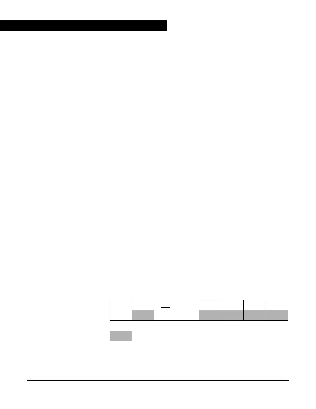
Address: $001D
Bit 7 654321Bit 0
Read:
AUTO
LOCK
ACQ XLD
0000
Write:
Reset: 0 0000000
=
Unimplemented
Figure 9-7. PLL Bandwidth Control Register (PBWC)
 Loading...


