Input/Output (I/O) Ports
Port C
MC68HC908AB32 — Rev. 1.0 Technical Data
MOTOROLA Input/Output (I/O) Ports 321
PTC[5:0] — Port C Data Bits
These read/write bits are software programmable. Data direction of
each port C pin is under the control of the corresponding bit in data
direction register C. Reset has no effect on port C data.
MCLK — T12 System Clock
The system clock is driven out of the PTC2 pin when MCLKEN is set.
17.5.2 Data Direction Register C (DDRC)
Data direction register C determines whether each port C pin is an input
or an output. Writing a logic 1 to a DDRC bit enables the output buffer
for the corresponding port C pin; a logic 0 disables the output buffer.
MCLKEN — T12 System Clock Enable Bit
This read/write bit enables MCLK to be an output signal on PTC2 pin.
Reset clears MCLKEN.
1 = PTC2 pin configured as MCLK output
0 = PTC2 pin configured as standard I/O pin
DDRC[5:0] — Data Direction Register C Bits
These read/write bits control port C data direction. Reset clears
DDRC[5:0], configuring all port C pins as inputs.
1 = Corresponding port C pin configured as output
0 = Corresponding port C pin configured as input
NOTE:
Avoid glitches on port C pins by writing to the port C data register before
changing data direction register C bits from 0 to 1. Figure 17-10 shows
the port C I/O logic.
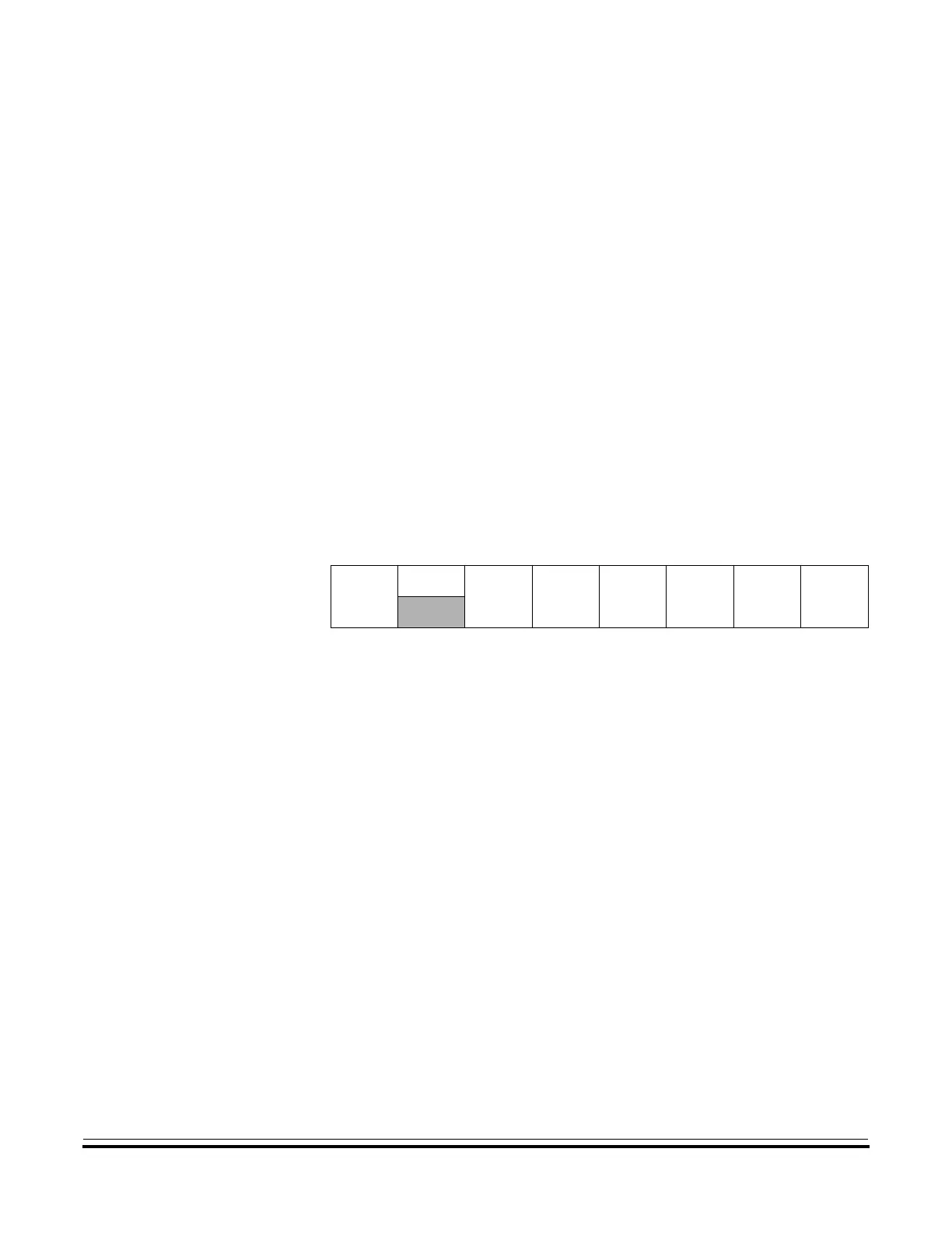
Address: $0006
Bit 7 654321Bit 0
Read:
MCLKEN
0
DDRC5 DDRC4 DDRC3 DDRC2 DDRC1 DDRC0
Write:
Reset: 0 0000000
Figure 17-9. Data Direction Register B (DDRB)
 Loading...


