Analog-to-Digital Converter (ADC)
I/O Registers
MC68HC908AB32 — Rev. 1.0 Technical Data
MOTOROLA Analog-to-Digital Converter (ADC) 237
14.8.2 ADC Data Register (ADR)
One 8-bit result register, ADC data register (ADR), is provided. This
register is updated each time an ADC conversion completes.
14.8.3 ADC Clock Register (ADCLK)
The ADC clock register (ADCLK) selects the clock frequency for the
ADC.
ADIV[2:0] — ADC Clock Prescaler Bits
ADIV[2:0] form a 3-bit field which selects the divide ratio used by the
ADC to generate the internal ADC clock. Table 14-2 shows the
available clock configurations. The ADC clock should be set to
approximately 1 MHz.
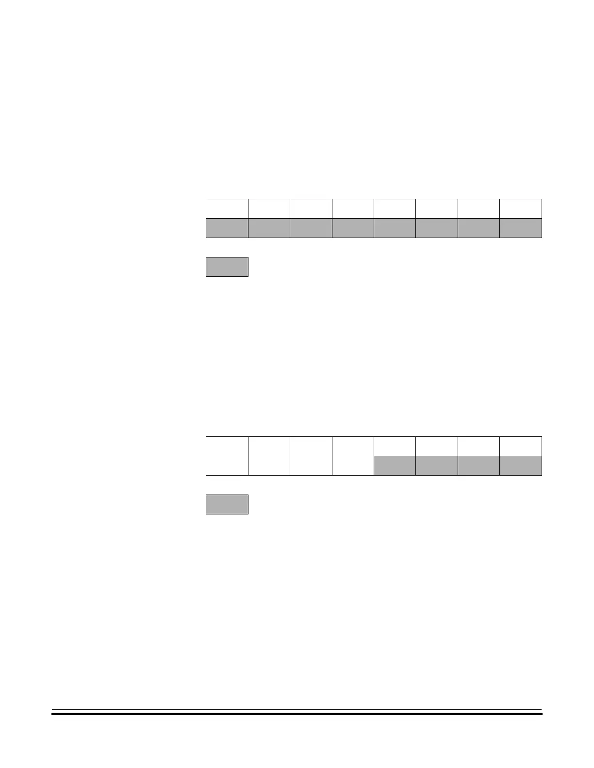
Address: $0039
Bit 7 654321Bit 0
Read: AD7 AD6 AD5 AD4 AD3 AD2 AD1 AD0
Write:
Reset: 00000000
= Unimplemented
Figure 14-4. ADC Data Register (ADR)
Address: $003A
Bit 7 654321Bit 0
Read:
ADIV2 ADIV1 ADIV0 ADICLK
0000
Write:
Reset: 00000000
= Unimplemented
Figure 14-5. ADC Clock Register (ADCLK)
 Loading...


