Electrical Specifications
ADC Characteristics
MC68HC908AB32 — Rev. 1.0 Technical Data
MOTOROLA Electrical Specifications 379
23.10 ADC Characteristics
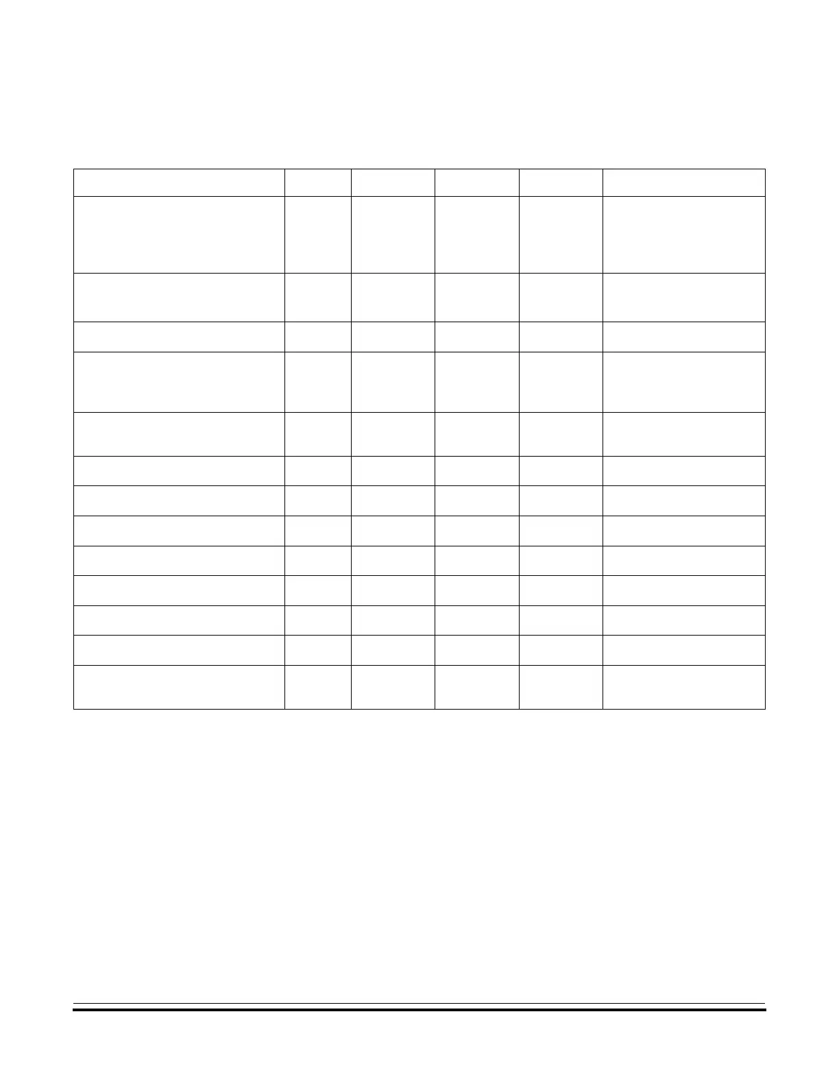
Characteristic
(1)
Symbol Min Max Unit Comments
Supply voltage
V
DDAD
4.5
(V
DD
min)
5.5
(V
DD
max)
V
V
DDAREF
should be tied
to the same potential as
V
DD
via separate
traces.
Input voltages
V
ADIN
V
REFH
0
1.5
V
DDAREF
V
DDAREF
V
V
ADIN
≤ V
REFH
Resolution
B
AD
8 8 Bits
Absolute accuracy
(V
REFL
= 0 V,
V
REFH
= V
DDAD
= 5 V ± 10%)
A
AD
± 1/2 ± 1 LSB Includes quantization
ADC internal clock
f
ADIC
0.5 1.048 MHz
t
AIC
= 1/f
ADIC
, tested
only at 1 MHz
Conversion range
R
AD
V
REFL
V
REFH
V
V
REFL
= V
SSA
Power-up time
t
ADPU
16
t
AIC
cycles
Conversion time
t
ADC
16 17
t
AIC
cycles
Sample time
(2)
t
ADS
5—
t
AIC
cycles
Zero input reading
(3)
Z
ADI
00 01 Hex
V
IN
= V
REFL
Full-scale reading
(3)
F
ADI
FE FF Hex
V
IN
= V
REFH
Input capacitance
C
ADI
— (20) 8 pF Not tested
Input leakage
(4)
Port B
—— ± 1 µA
Notes:
1. V
DD
= 5.0 Vdc ± 10%, V
DDA
= V
DDAREF
= 5.0 Vdc ± 10%, V
REFH
= 5.0 Vdc ± 10%, V
SS
= 0 Vdc, V
REFL
= V
SSA
= 0 Vdc
2. Source impedances greater than 10 kΩ adversely affect internal RC charging time during input sampling.
3. Zero-input/full-scale reading requires sufficient decoupling measures for accurate conversions.
4. The external system error caused by input leakage current is approximately equal to the product of R source and input
current.
 Loading...


