Input/Output (I/O) Ports
Port B
MC68HC908AB32 — Rev. 1.0 Technical Data
MOTOROLA Input/Output (I/O) Ports 319
17.4.2 Data Direction Register B (DDRB)
Data direction register B determines whether each port B pin is an input
or an output. Writing a logic 1 to a DDRB bit enables the output buffer for
the corresponding port B pin; a logic 0 disables the output buffer.
DDRB[7:0] — Data Direction Register B Bits
These read/write bits control port B data direction. Reset clears
DDRB[7:0], configuring all port B pins as inputs.
1 = Corresponding port B pin configured as output
0 = Corresponding port B pin configured as input
NOTE:
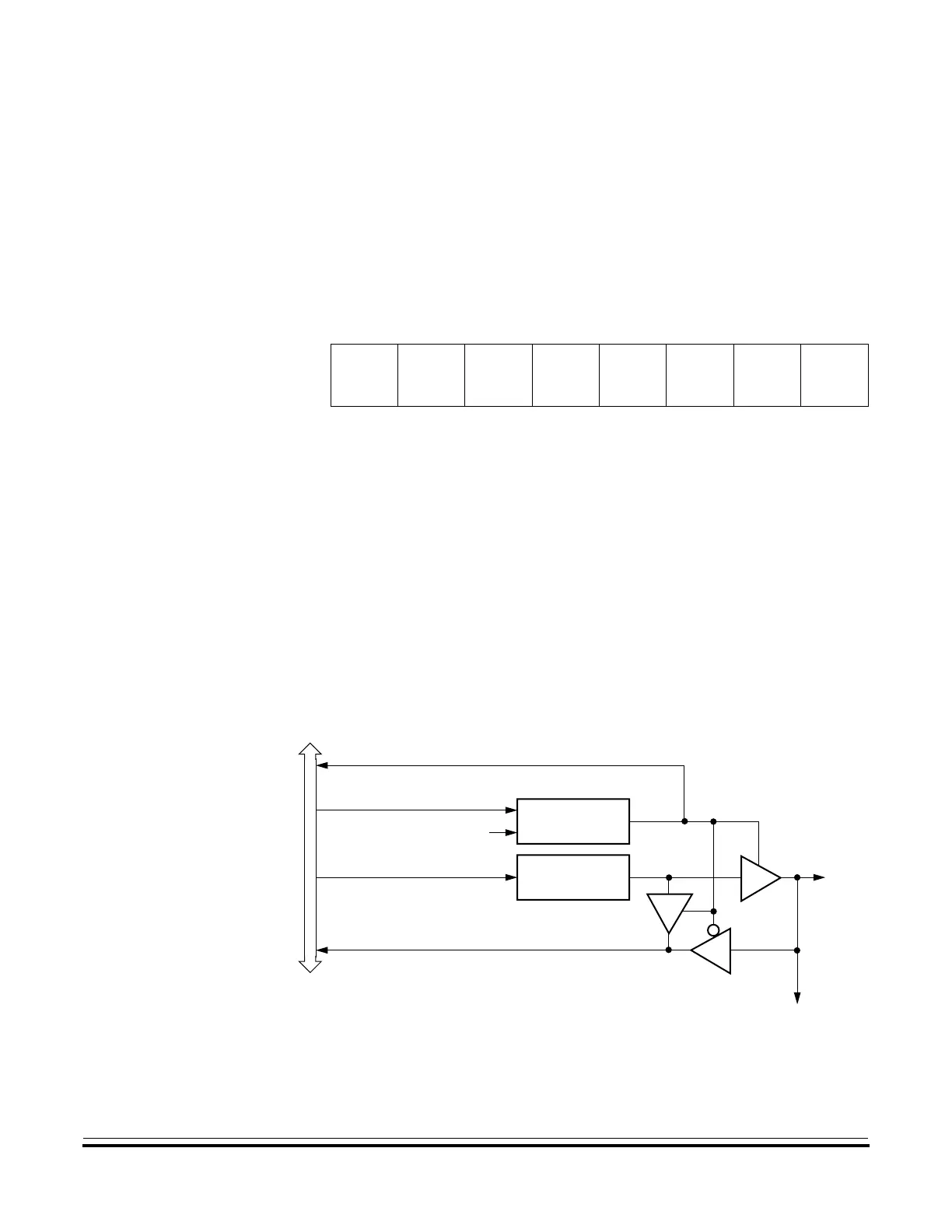
Avoid glitches on port B pins by writing to the port B data register before
changing data direction register B bits from 0 to 1. Figure 17-7 shows
the port B I/O logic.
Figure 17-7. Port B I/O Circuit
Address: $0005
Bit 7 654321Bit 0
Read:
DDRB7 DDRB6 DDRB5 DDRB4 DDRB3 DDRB2 DDRB1 DDRB0
Write:
Reset: 0 0000000
Figure 17-6. Data Direction Register B (DDRB)
READ DDRB ($0005)
WRITE DDRB ($0005)
RESET
WRITE PTB ($0001)
READ PTB ($0001)
PTBx
DDRBx
PTBx
INTERNAL DATA BUS
To Analog-To-Digital Converter
 Loading...


