Input/Output (I/O) Ports
Port D
MC68HC908AB32 — Rev. 1.0 Technical Data
MOTOROLA Input/Output (I/O) Ports 325
When DDRDx is a logic 1, reading address $0003 reads the PTDx data
latch. When DDRDx is a logic 0, reading address $0003 reads the
voltage level on the pin. The data latch can always be written, regardless
of the state of its data direction bit.
Table 17-5 summarizes the operation of the port D pins.
17.6.3 Port D Input Pullup Enable Register (PTDPUE)
The port D input pullup enable register (PTDPUE) controls the input
pullup device for each of the eight port D pins. Each bit is individually
configurable and requires that the data direction register, DDRD, bit be
configured as an input. Each pullup is automatically and dynamically
disabled when a port bit’s DDRD is configured for output mode.
PTDPUE[7:0] — Port D Input Pullup Enable Bits
These writable bits are software programmable to enable pullup
devices on an input port pin.
1 = Corresponding port D pin configured to have internal pullup
0 = Corresponding port D pin internal pullup disconnected
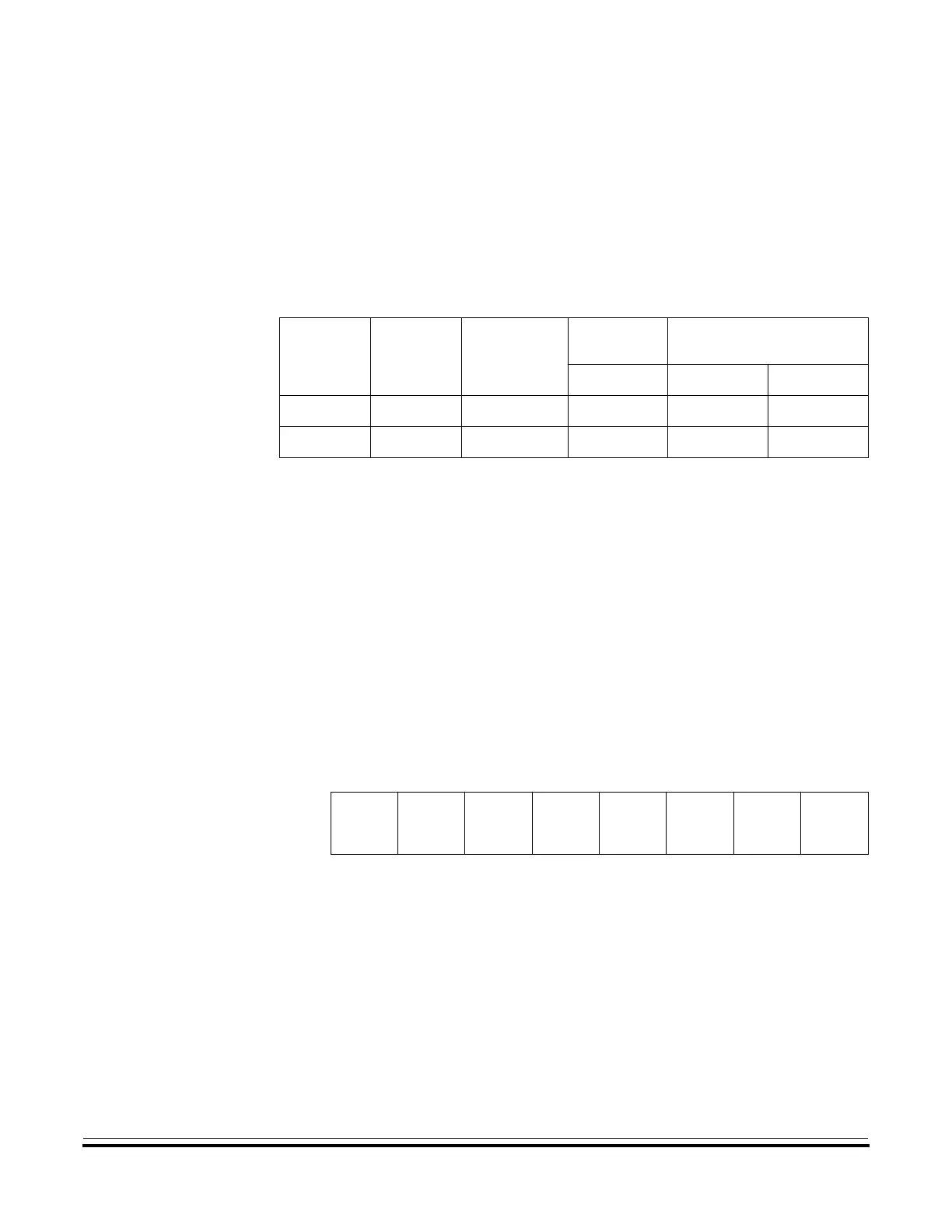
Table 17-5. Port D Pin Functions
DDRD
Bit
PTD Bit
I/O Pin
Mode
Accesses
to DDRD
Accesses to PTD
Read/Write Read Write
0X
(1)
Notes:
1. X = don’t care.
Input, Hi-Z
(2)
2. Hi-Z = high impedance.
DDRD[7:0] Pin PTD[7:0]
(3)
3. Writing affects data register, but does not affect the input.
1 X Output DDRD[7:0] PTD[7:0] PTD[7:0]
Address: $003D
Bit 7 654321Bit 0
Read:
PTDPUE7 PTDPUE6 PTDPUE5 PTDPUE4 PTDPUE3 PTDPUE2 PTDPUE1 PTDPUE0
Write:
Reset: 0 0000000
Figure 17-14. Port D Input Pullup Enable Register (PTDPUE)
 Loading...


