Clock Generator Module (CGM)
Technical Data MC68HC908AB32 — Rev. 1.0
144 Clock Generator Module (CGM) MOTOROLA
9.6.1 PLL Control Register (PCTL)
The PLL control register contains the interrupt enable and flag bits, the
on/off switch, and the base clock selector bit.
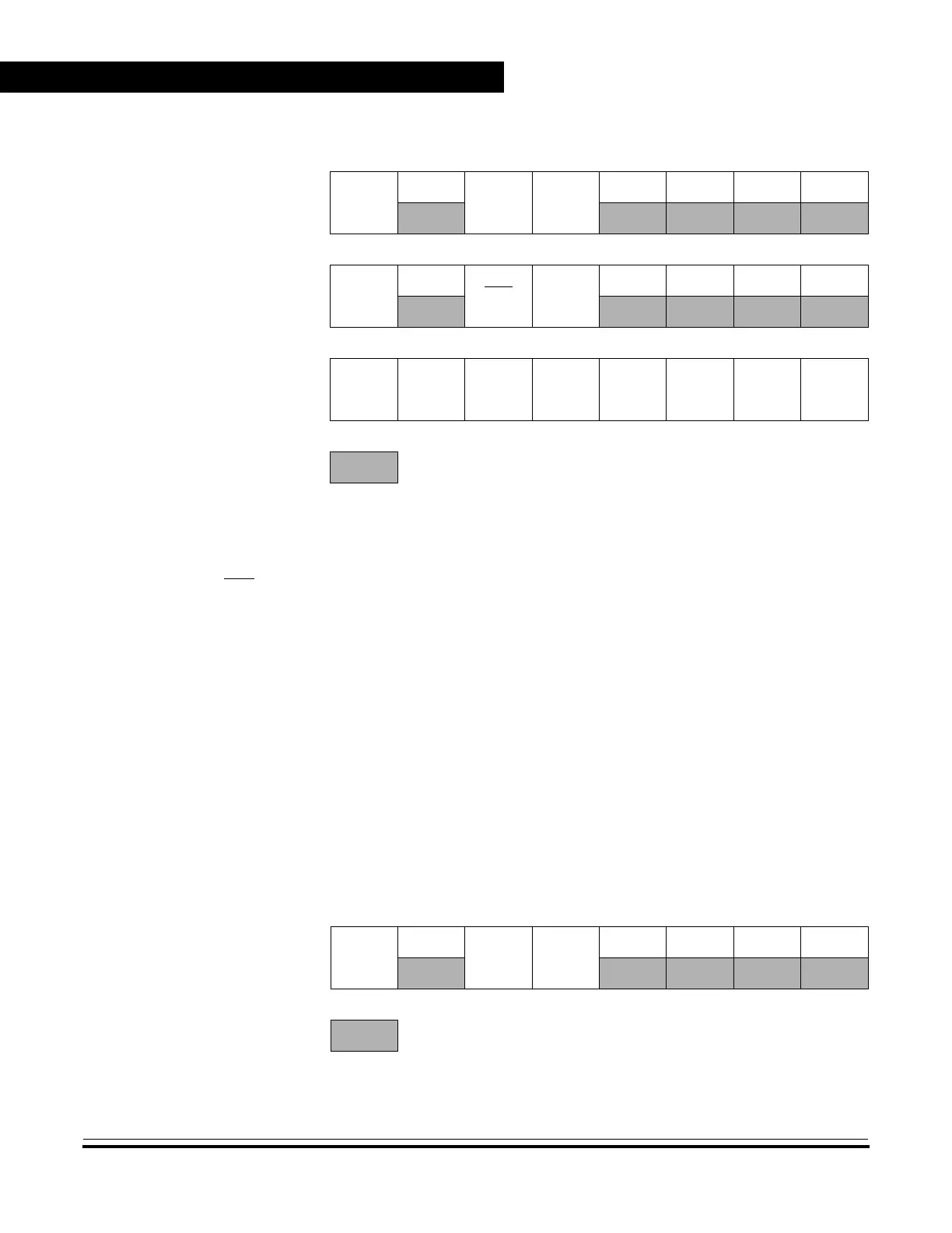
Addr. Register Name Bit 7 654321Bit 0
$001C
PLL Control Register
(PCTL)
Read:
PLLIE
PLLF
PLLON BCS
1111
Write:
Reset: 00101111
$001D
PLL Bandwidth Control
Register
(PBWC)
Read:
AUTO
LOCK
ACQ XLD
0000
Write:
Reset: 00000000
$001E
PLL Programming
Register
(PPG)
Read:
MUL7 MUL6 MUL5 MUL4 VRS7 VRS6 VRS5 VRS4
Write:
Reset: 01100110
= Unimplemented
NOTES:
1. When AUTO = 0, PLLIE is forced to logic zero and is read-only.
2. When AUTO = 0, PLLF and LOCK read as logic zero.
3. When AUTO = 1, ACQ
is read-only.
4. When PLLON = 0 or VRS[7:4] = $0, BCS is forced to logic zero and is read-only.
5. When PLLON = 1, the PLL programming register is read-only.
6. When BCS = 1, PLLON is forced set and is read-only.
Figure 9-4. CGM I/O Register Summary
Address: $001C
Bit 7 654321Bit 0
Read:
PLLIE
PLLF
PLLON BCS
1111
Write:
Reset: 0 0101111
=
Unimplemented
Figure 9-5. PLL Control Register (PCTL)
 Loading...


