Input/Output (I/O) Ports
Port G
MC68HC908AB32 — Rev. 1.0 Technical Data
MOTOROLA Input/Output (I/O) Ports 333
PTG[2:0] — Port G Data Bits
These read/write bits are software programmable. Data direction of
each port G pin is under the control of the corresponding bit in data
direction register G. Reset has no effect on port G data.
KBD[2:0] — The keyboard interrupt enable bits, KBIE[2:0], in the
keyboard interrupt enable register (KBIER), enable the port G pins as
external interrupt pins. See Section 19. Keyboard Interrupt Module
(KBI).
17.9.2 Data Direction Register G (DDRG)
Data direction register G determines whether each port G pin is an input
or an output. Writing logic 1 to a DDRG bit enables the output buffer for
the corresponding port G pin; a logic 0 disables the output buffer.
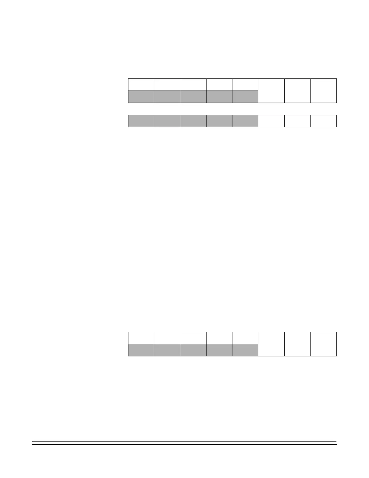
Address: $000A
Bit 7 654321Bit 0
Read: 00000
PTG2 PTG1 PTG0
Write:
Reset: Unaffected by reset
Alternative Function: KBD2 KBD1 KBD0
Figure 17-22. Port G Data Register (PTG)
Address: $000E
Bit 7 654321Bit 0
Read: 0 0000
DDRG2 DDRG1 DDRG0
Write:
Reset: 0 0000000
Figure 17-23. Data Direction Register G (DDRG)
 Loading...


