Clock Generator Module (CGM)
Technical Data MC68HC908AB32 — Rev. 1.0
134 Clock Generator Module (CGM) MOTOROLA
9.4.1 Crystal Oscillator Circuit
The crystal oscillator circuit consists of an inverting amplifier and an
external crystal. The OSC1 pin is the input to the amplifier and the OSC2
pin is the output. The SIMOSCEN signal from the system integration
module (SIM) enables the crystal oscillator circuit.
The CGMXCLK signal is the output of the crystal oscillator circuit and
runs at a rate equal to the crystal frequency. CGMXCLK is then buffered
to produce CGMRCLK, the PLL reference clock.
CGMXCLK can be used by other modules which require precise timing
for operation. The duty cycle of CGMXCLK is not guaranteed to be 50%
and depends on external factors, including the crystal and related
external components.
An externally generated clock can also feed the OSC1 pin of the crystal
oscillator circuit. For this configuration, the external clock should be
connected to the OSC1 pin and the OSC2 pin allowed to float.
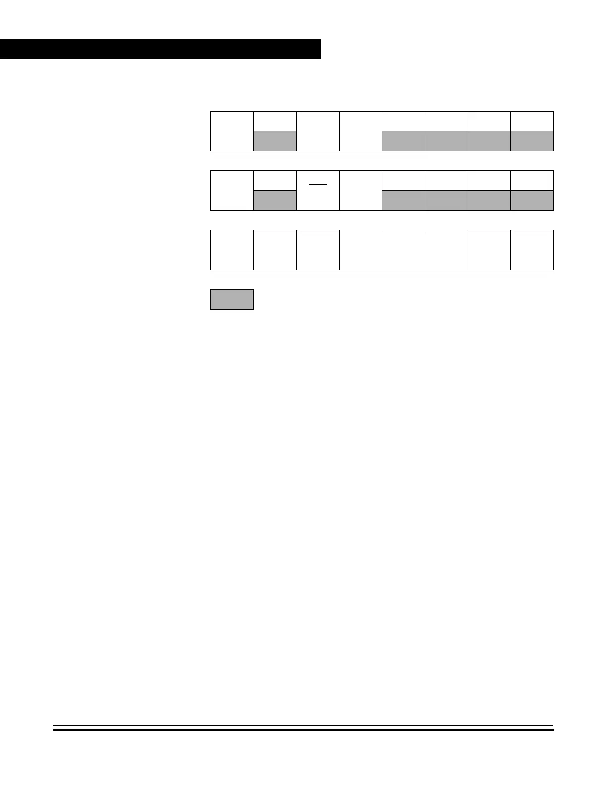
Addr. Register Name Bit 7 654321Bit 0
$001C
PLL Control Register
(PCTL)
Read:
PLLIE
PLLF
PLLON BCS
1111
Write:
Reset: 00101111
$001D
PLL Bandwidth Control
Register
(PBWC)
Read:
AUTO
LOCK
ACQ XLD
0000
Write:
Reset: 00000000
$001E
PLL Programming
Register
(PPG)
Read:
MUL7 MUL6 MUL5 MUL4 VRS7 VRS6 VRS5 VRS4
Write:
Reset: 01100110
= Unimplemented
Figure 9-2. CGM I/O Register Summary
 Loading...


