Input/Output (I/O) Ports
Technical Data MC68HC908AB32 — Rev. 1.0
330 Input/Output (I/O) Ports MOTOROLA
PTF[7:0] — Port F Data Bits
These read/write bits are software programmable. Data direction of
each port F pin is under the control of the corresponding bit in data
direction register F. Reset has no effect on port F data.
TACH[3:2] and TBCH[3:0] — Timer channel I/O bits
The PTF5/TBCH1–PTF0/TACH2 pins are the TIMA and TIMB input
capture/output compare pins. The edge/level select bits,
ELSxB:ELSxA, determine whether the PTF5/TBCH1–PTF0/TACH2
pins are timer channel I/O pins or general-purpose I/O pins. See
11.10.4 TIMA Channel Status and Control Registers and 12.10.4
TIMB Channel Status and Control Registers.
NOTE:
Data direction register F (DDRF) does not affect the data direction of
port F pins that are being used by TIMA and TIMB. However, the DDRF
bits always determine whether reading port F returns the states of the
latches or the states of the pins. See Table 17-7.
17.8.2 Data Direction Register F (DDRF)
Data direction register F determines whether each port F pin is an input
or an output. Writing a logic 1 to a DDRF bit enables the output buffer for
the corresponding port F pin; a logic 0 disables the output buffer.
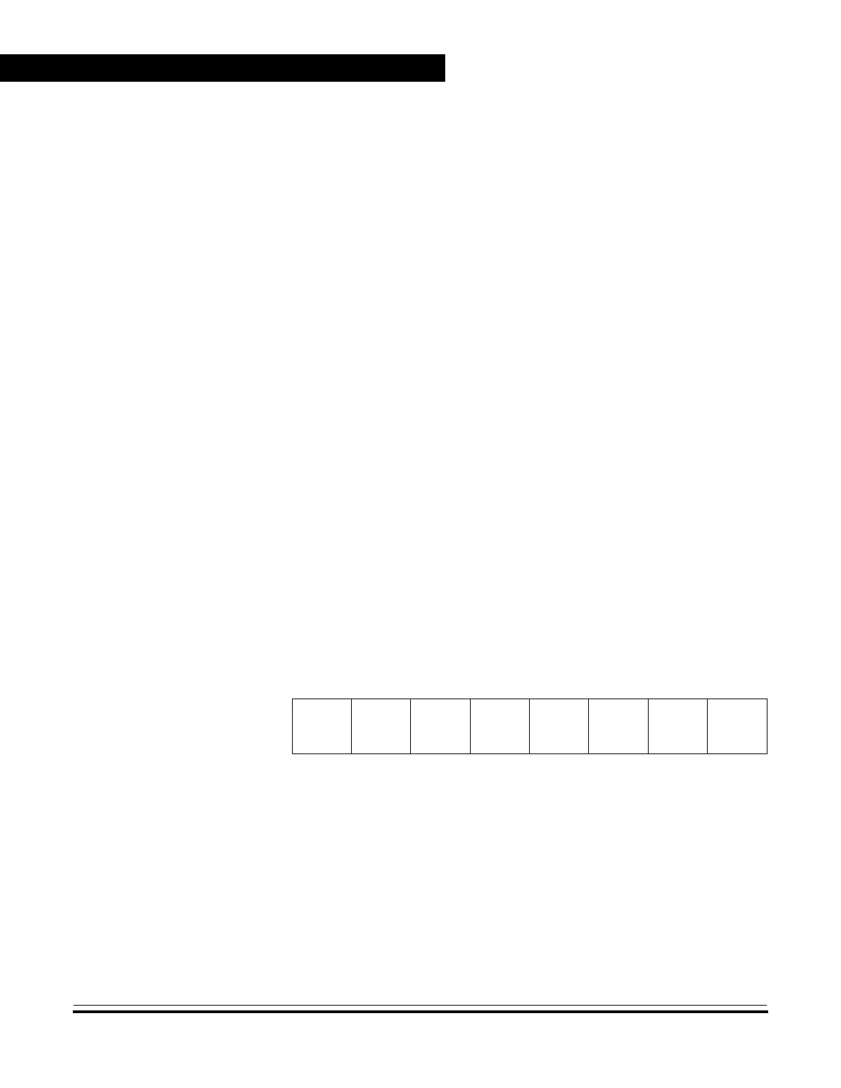
DDRF[7:0] — Data Direction Register F Bits
These read/write bits control port F data direction. Reset clears
DDRF[7:0], configuring all port F pins as inputs.
1 = Corresponding port F pin configured as output
0 = Corresponding port F pin configured as input
Address: $000D
Bit 7 654321Bit 0
Read:
DDRF7 DDRF6 DDRF5 DDRF4 DDRF3 DDRF2 DDRF1 DDRF0
Write:
Reset: 0 0000000
Figure 17-19. Data Direction Register F (DDRF)
 Loading...


