10 Memory Interface
10 – 26
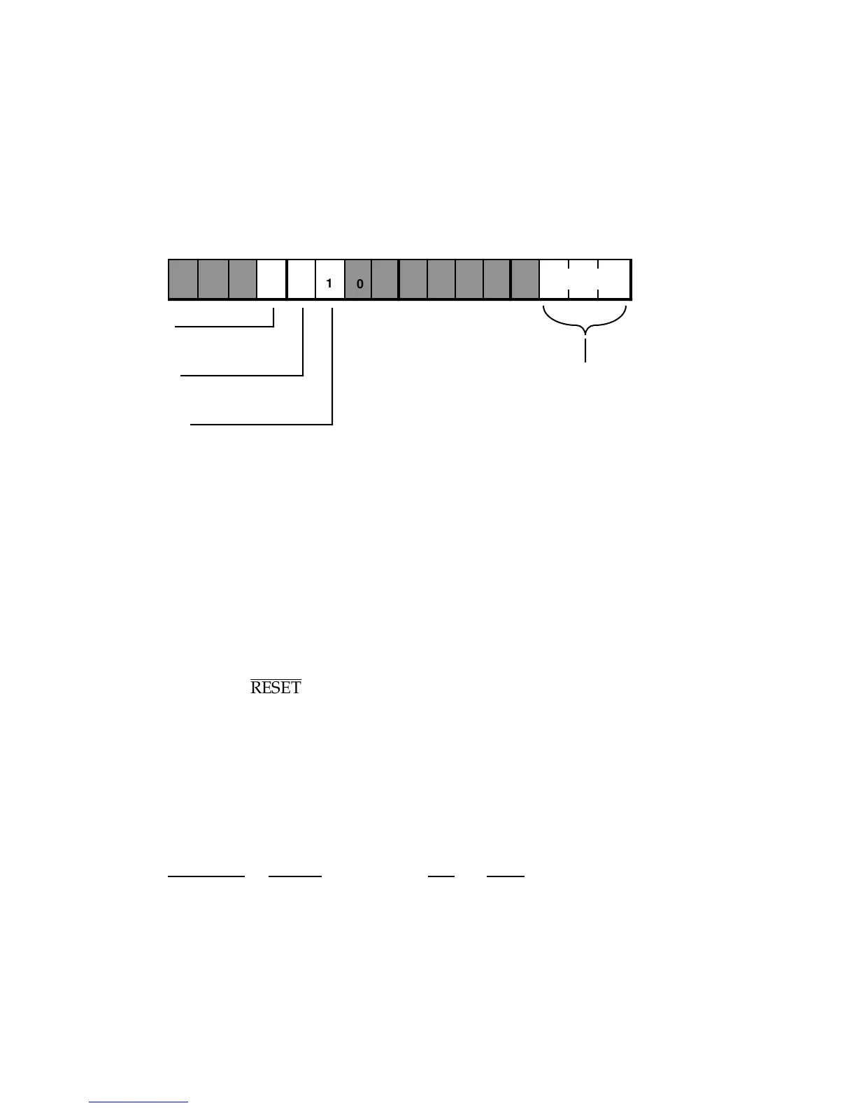
Figure 10.24 PWAIT Field in System Control Register
The on-chip program memory and overlays can hold instructions and
data intermixed in any combination. The ADSP-21xx linker determines
where to place relocatable code and data segments. You may specify
absolute address placement for any module or data structure, including
the code for the restart and interrupt vector locations. The restart vector is
at program memory address 0x0000.
The ADSP-2181’s MMAP pin lets you select from two program memory
configurations. The MMAP pin also controls whether the ADSP-2181
boots after
RESET
is released. Figure 10.25 shows the MMAP options and
the resulting memory maps for program memory.
The program memory overlay select register (PMOVLAY) lets you choose
a memory overlay to map from address PM(0x2000) to address
PM(0x3FFF). The memory mapped to this space and corresponding
PMOVLAY register values are shown in Figure 10.25. Table 10.3 shows
how PMOVLAY relates to the addressing of memory locations (with
address line A13).
PMOVLAY Memory A13 A12:0
0 Internal — —
1 External overlay 1 0 13 LSBs of address between
0x2000 and 0x3FFF
2 External overlay 2 1 13 LSBs of address between
0x2000 and 0x3FFF
Table 10.3 PMOVLAY and Program Memory Overlay Addressing
1514131211109876543210
PWAIT
Program Memory Overlay Wait States
0
100
DM (0x3FFF)
SPORT1 Enable
1 = enabled, 0 = disabled
SPORT1 Configure
1 = serial port
0 = FI, FO, IRQ0, IRQ1, SCLK
000
111
11000
00 000 00
System Control Register
SPORT0 Enable
1 = enabled, 0 = disabled

 Loading...

