10 Memory Interface
10 – 28
ADSP-2100 family processors.
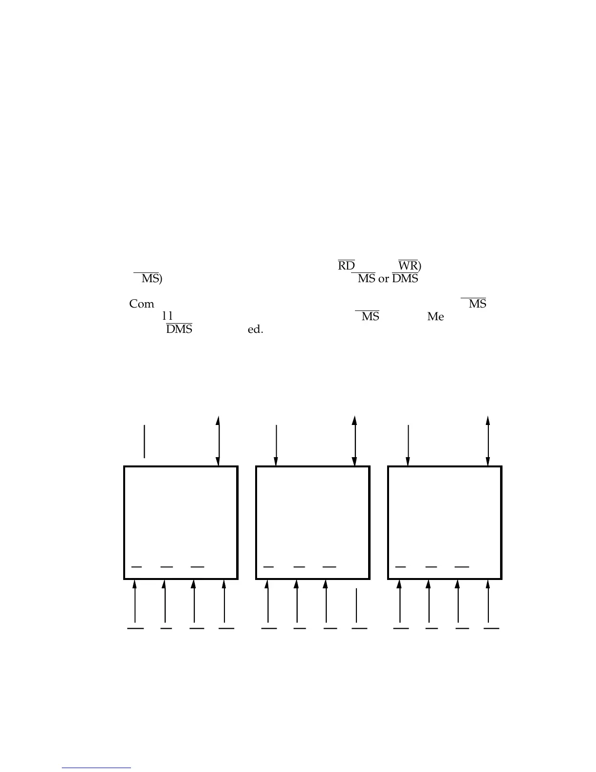
Figure 10.26 shows a memory design that provides full external program
and data memory overlays for an ADSP-2181 processor, assuming that
MMAP=0. The important points to note about this design are:
• Three 32K x 8-bit SRAMs are required for full external program and
data memory overlays; glue logic is not required.
• Four control lines are required for read (
RD
), write (
WR
), chip select
(
CMS
), and data/program memory select (
PMS
or
DMS
).
• Composite Memory Select (CMSSEL) is configured to assert the
CMS
control line when Program Memory Select (
PMS
) or Data Memory
Select (
DMS
) are asserted.
• The order of overlays stored in this design (from lowest address to
highest) is PM Overlay 1, PM Overlay 2, DM Overlay 1, and DM
Overlay 2. Address line 13 (A13) of the ADSP-2181 selects between
overlay 1 or 2. Figure 10.27 shows a memory map of this design.
A14 A14
A0 - 13 D0 - 7
CS
OE WE
CMS RD WR
A0 - 13 D0 - 7
CS
OE WE
CMS RD WR
A0 - 13 D0 - 7
CS
OE WE
CMS RD WRPMS
A14
32K x 8 BIT
SRAM
32K x 8 BIT
SRAM
32K x 8 BIT
SRAM
ADDR 0 - 13
DATA 0 - 7
ADDR 0 - 13
DATA 8 - 15
ADDR 0 - 13
DATA 16 - 23
PMS PMS
Figure 10.26 Example Program and Data Memory Overlay Design

 Loading...

