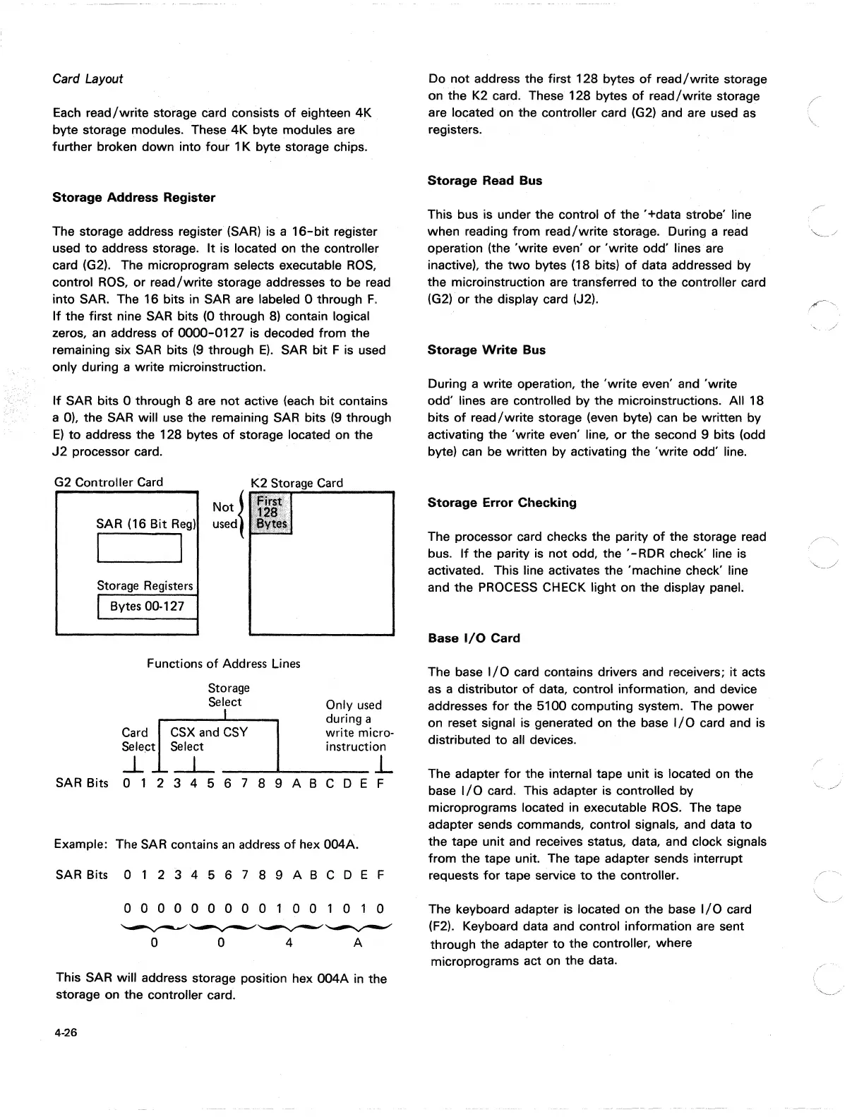
Card Layout
Each
read/write
storage card consists
of
eighteen
4K
byte storage modules. These
4K
byte modules are
further broken down into four 1 K byte storage chips.
Storage
Address
Register
The storage address register (SAR) is a
16-bit
register
used
to
address storage.
It
is located on the controller
card (G2). The microprogram selects executable
ROS,
control
ROS,
or
read/write
storage addresses
to
be
read
into SAR. The 16 bits
in
SAR are labeled 0 through
F.
If
the first nine SAR bits (0 through
8)
contain logical
zeros,
an
address
of
0000-0127 is decoded from the
remaining six SAR bits
(9
through
E).
SAR bit F is used
only during a write microinstruction.
If
SAR bits 0 through 8 are not active (each bit contains
a
0),
the SAR will use the remaining SAR bits
(9
through
E)
to
address the 128 bytes
of
storage located on the
J2
processor card.
G2 Controller
Card
Not
{ K2
Storage
Card
SAR (16
Bit
Reg)
I I
Storage
Registers
I Bytes 00-127
used
Functions
of
Address
Lines
Storage
Select
Only
used
during a
Card
CSX
and
CSY
write micro-
Sele~t
Select instruction
.l..
-L
_~
___
.L
SAR Bits 0 1 2 3 4 5 6 7 8 9
ABC
D E F
Example: The SAR contains
an
address
of
hex 004A.
SAR Bits 0
234
5 6 7 8 9
ABC
D E F
o 0 0 0 0 0
000
00101
0
~~~~
o 0 4 A
This SAR will address storage position hex oo4A
in
the
storage on the controller card.
4-26
Do not address the first 128 bytes
of
read/write
storage
on the
K2
card. These 128 bytes
of
read/write
storage
are located on the controller card
(G2)
and are used
as
registers.
Storage
Read Bus
This bus is under the control
of
the'
+data strobe' line
when reading from
read/write
storage. During a read
operation (the
'write
even' or
'write
odd' lines
are
inactive), the
two
bytes (18 bits)
of
data addressed by
the microinstruction are transferred
to
the controller card
(G2)
or the display card (J2).
Storage
Write
Bus
During a write operation, the
'write
even' and
'write
odd' lines are controlled by the microinstructions. All 18
bits
of
read/write
storage (even byte) can be written by
activating the
'write
even' line,
or
the second 9 bits (odd
byte) can
be
written by activating the
'write
odd' line.
Storage
Error
Checking
The processor card checks the parity
of
the storage read
bus.
If
the parity is not odd, the
'-RDR
check' line
is
activated. This line activates the 'machine check' line
and the
PROCESS
CHECK light on the display panel.
Base
I/O
Card
The base
I/O
card contains drivers and receivers;
it
acts
as
a distributor
of
data, control information, and device
addresses
for
the 5100 computing system. The power
on reset signal
is
generated on the base
I/O
card and is
distributed
to
all devices.
The adapter
for
the internal tape unit is located
on
the
base
I/O
card. This adapter is controlled by
microprograms located
in
executable
ROS.
The tape
adapter sends commands, control signals, and data
to
the tape unit and receives status, data, and clock signals
from
the tape unit. The tape adapter sends interrupt
requests
for
tape service
to
the controller.
The keyboard adapter is located on the base
I/O
card
(F2).
Keyboard data and control information are sent
through the adapter
to
the controller, where
microprograms act
on
the data.
 Loading...