(
(
(.
-
.-
/
(
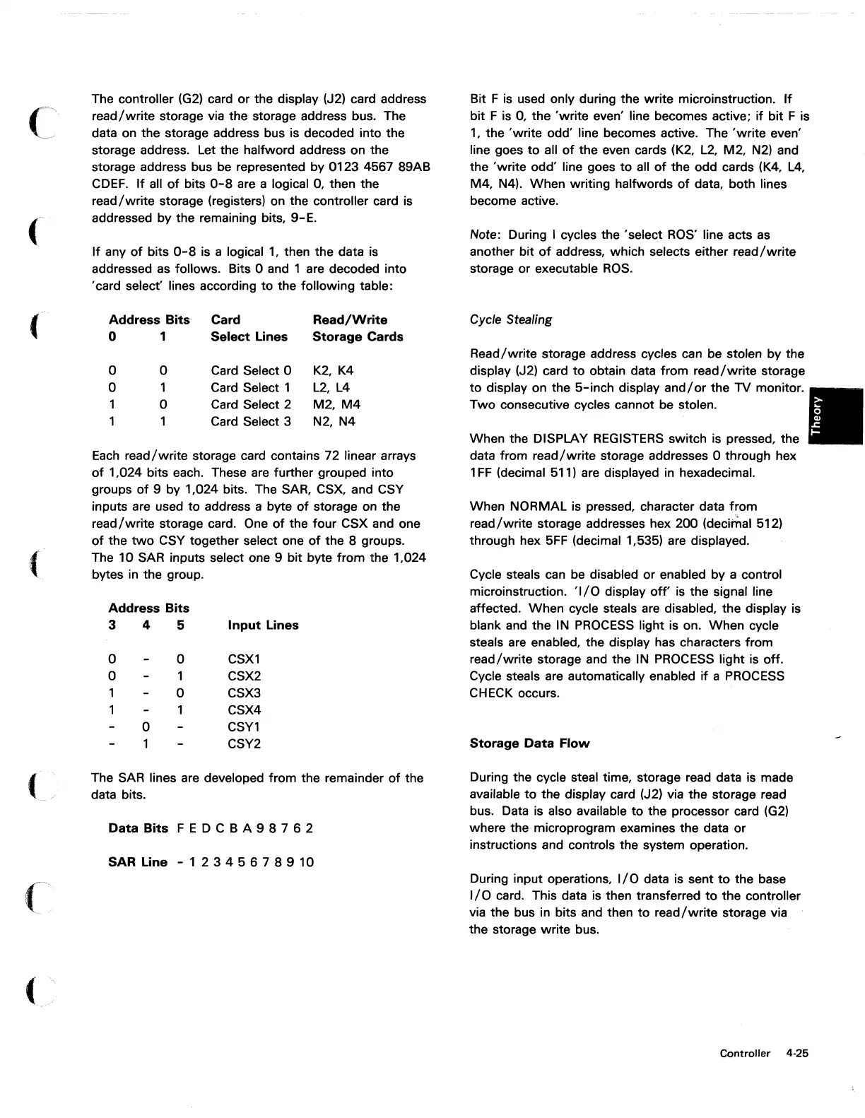
The controller
(G2)
card or the display (J2) card address
read/write
storage via the storage address bus. The
data on the storage address bus is decoded into the
storage address. Let the halfword address on the
storage address bus be represented by 0123 4567 89AB
CDEF.
If
all
of
bits
0-8
are a logical 0, then the
read/write
storage (registers) on the controller card
is
addressed
by
the remaining bits, 9-E.
If
any
of
bits
0-8
is a logical
1,
then the data is
addressed
as
follows. Bits 0 and 1 are decoded into
'card select' lines according
to
the following table:
Address
Bits
Card
Read/Write
0
1
Select
Lines
Storage
Cards
0 0
Card Select 0
K2,
K4
0 Card Select 1
L2,
L4
1 0 Card Select 2
M2,
M4
1
Card Select 3
N2, N4
Each
read/write
storage card contains 72 linear arrays
of
1,024 bits each. These are further grouped into
groups
of
9 by 1,024 bits. The SAR, CSX, and CSY
inputs are used
to
address a byte
of
storage on the
read/write
storage card.
One
of
the four CSX and one
of
the
two
CSY together select one
of
the 8 groups.
The 10 SAR inputs select one 9 bit byte
from
the 1,024
bytes
in
the group.
Address
Bits
345
o
o
o
o
1
o
Input
Lines
CSX1
CSX2
CSX3
CSX4
CSY1
CSY2
The SAR lines are developed from the remainder
of
the
data bits.
Data
Bits
FED
C B A 9 8 7 6 2
SAR
Line - 1 2 3 4 5 6 7 8 9 10
Bit F
is
used only during the write microinstruction.
If
bit F is 0,
the
'write
even' line becomes active;
if
bit
F is
1,
the
'write
odd' line becomes active. The
'write
even'
line goes
to
all
of
the even cards (K2,
L2,
M2,
N2)
and
the
'write
odd' line goes
to
all
of
the odd cards (K4,
L4,
M4, N4). When writing halfwords
of
data, both lines
become active.
Note: During I cycles the 'select ROS' line acts
as
another bit
of
address, which selects either
read/write
storage or executable
ROS.
Cycle Stealing
Read/write storage address cycles can be stolen by the
display (J2) card
to
obtain data from
read/write
storage
to
display on the
5-inch
display
and/or
the TV monitor.
Two consecutive cycles cannot be stolen.
When the DISPLAY REGISTERS switch is pressed, the
data from
read/write
storage addresses 0 through hex
1
FF
(decimal 511) are displayed
in
hexadecimal.
When NORMAL is pressed, character data
from
read/write
storage addresses hex 200 (decimal 512)
through hex
5FF
(decimal 1,535) are displayed.
Cycle steals
can
be disabled
or
enabled by a control
microinstruction.
'I/O
display
off'
is
the signal line
affected. When cycle steals are disabled, the display
is
blank and the IN
PROCESS
light is on. When cycle
steals
are
enabled, the display has characters from
read/write
storage and the
IN
PROCESS light is off.
Cycle steals are automatically enabled
if
a
PROCESS
CHECK occurs.
Storage
Data
Flow
During the cycle steal time, storage read data is made
available
to
the display card (J2) via the storage read
bus. Data is also available
to
the processor card
(G2)
where the microprogram examines the data or
instructions and controls the system operation.
During input operations,
I/O
data is sent
to
the base
I/O
card. This data is then transferred
to
the controller
via the bus in bits and then
to
read/write
storage via
the storage write bus.
Controller 4-25
 Loading...