Read/Write Storage Addressing
D
..
tJ
If)
II
SARBus
II
..
'
+CSY1
+CSY2·
+CSX1
-
A
;---
----
+CSX2
~
+CSX3
r-L}
+CSX4
A
+Card Select
+Write Data
r
1
t----
r
1
~
r-
1
L--
r
1
1
LN
Read Data
Write Bus
l....-
p'
o.
II
II
A
IJ
II
A
IJ
A
II
.'
A
II
A
II
A
IJ
A
fJ
A
II
p
0
I SA
SA
I
I
-.
l'
2'
31;415161
7'
II
II.
II
II
II
II
II
Each
row
is 1 K
bytes
of
data
I
I
II
SAR
and
Card
L
Select I
1---.1
CSX
I
~
V:L
I I
I
Read Data I
.
I
.
I
I
200 ns
400
ns
1
2
3 4
5
6
7 Storage Cycle
SA
SA
SA SA
SA
SA
SA
} Sense Amplifiers
I
I
I I
I I
I
Read Bus
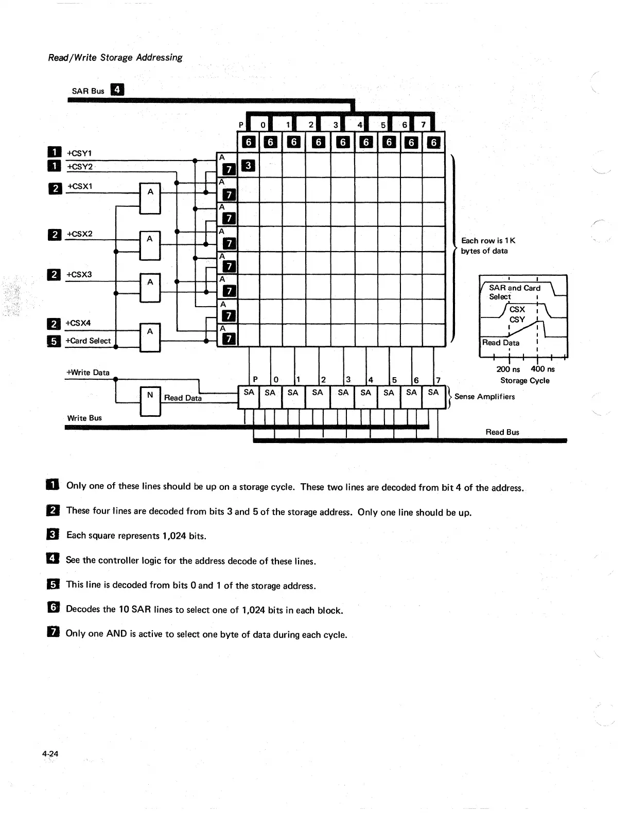
D Only one
of
these lines should
be
up on a storage cycle. These two lines are decoded from bit 4 of the address.
fJ
These four lines are decoded from bits 3 and 5
of
the storage address. Only one line should be up.
D Each square represents 1,024 bits.
D See the controller logic for the address decode
of
these lines.
1.1
This line
is
decoded from bits 0 and 1
of
the storage address.
II
Decodes the 10 SAR lines
to
select one of 1,024 bits
in
each block.
fJ
Only one
AND
is
active
to
select one byte of data during each cycle.
 Loading...