101
9−2−5.
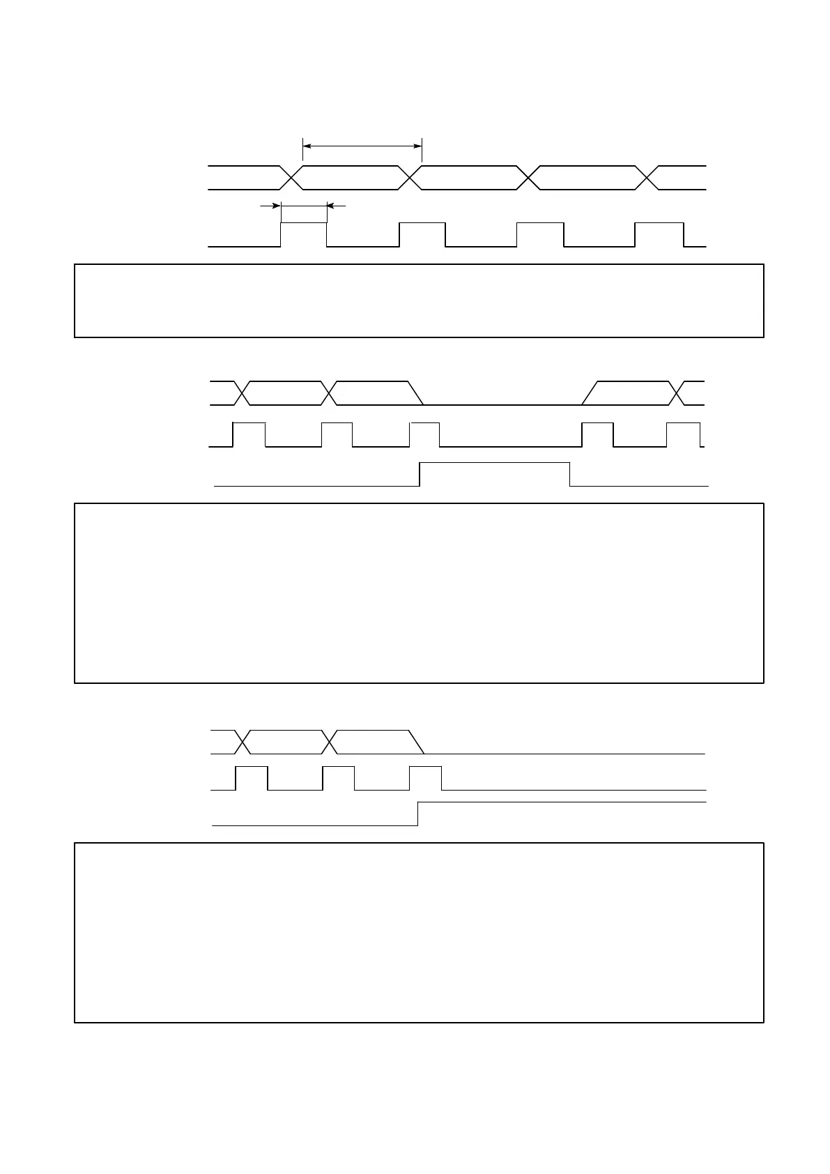
Timing chart
(1)
Normal
DATA
POL.
20 times/s : Approx. 50 ms
4 times/s : Approx. 250 ms
ON
P.C.
4 times/s : Approx. 25 ms/125 ms changeable
20 times/s : Approx. 25 ms
ON ON
ONONON
ON
ON
● At the time of data output each of P.C., DATA and POL, output
transistor will become ON. (Negative logic electrically.)
(2)
When the data is overranged
DATA
POL.
P.C.
OVR.
ON
ON ON
ON
ON
ON
● At the time of OVR output, output transistor at OVR signal will
become ON(Negative logic electrically). Moreover, for each P.C., and
DATA, output transistor will become OFF(Positive logic electrically)
at the time of OVR output is applied.
(However, only for P.C., OFF condition is made after one(1) shot of
operation and POL is always ON.)
(3)
When ERROR is occurred.
DATA
POL.
P.C.
ERROR
ON
ON
ON
ON
● At the time of ERROR output, output transistor at ERROR signal
will become ON(Negative logic electrically). Moreover, for each P.C.,
DATA and POL, output transistor will become OFF(Positive logic
electrically) at the time of ERROR output is applied. (However, only
for P.C., OFF condition is made after one(1) pulse of operation is
finished).