Chapter 7
I/O Port
VII - 36 Port 0
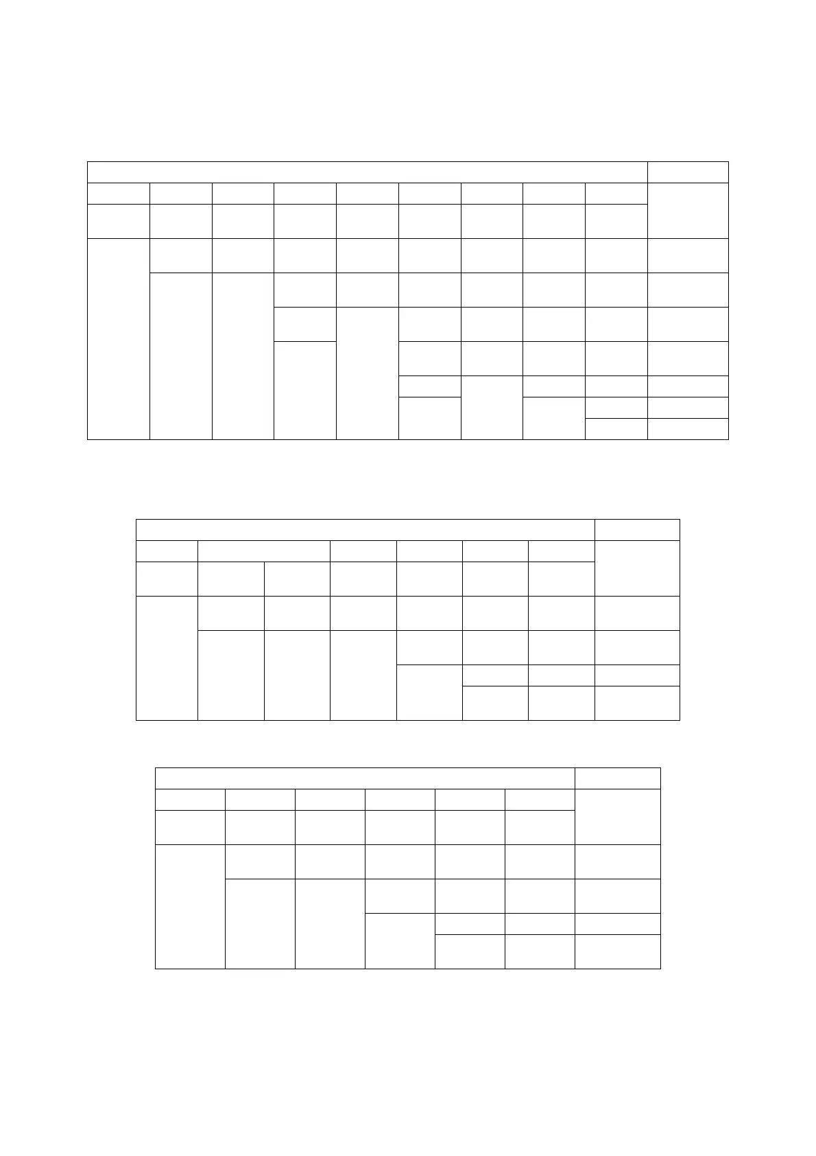
Table:7.4.7 P05 Function Selection
*1 When the LSI is the master of Clock-synchronous communication or communicates on IIC bus,
set the P0DIR.P0DIR5 to "1".
Table:7.4.8 P06 Function Selection
Table:7.4.9 P07 Function Selection
*1 When the LSI outputs the chip select signal, set the P0DIR.P0DIR7 to "1".
Setup Function
Register SC3MD1 SC23SEL TM0MD TMIOEN0 TM2MD TMIOEN0 TMIOSEL0 CLKOUT
Bit name SC3SBTS SC3SEL2 TM0CK1-0 TM0OEN TM2CK1-0 TM2OEN
TM0IOSE/
TM2IOSEL
CLKOEN/
CLKOSEL
1 (*1) 0
Other than
11
0
Other than
11
0 -/- 0/- SBT3A/SCL3A
0-
Other than
11
1
Other than
11
0 0/- 0/- TM0IO (output)
11
0
Other than
11
0 0/- 0/- TM0IO (input)
Other than
11
Other than
11
1 -/0 0/- TM2IO (output)
11
0
-/0 0/- TM2IO (input)
Other than
11
-/-
1/0 CLKOUTA
0/- P05
Setup Function
Register SC3MD1 SC23SEL TMIOEN1 TM8MD1 TMIOSEL1
Bit name SC3SBIS SC3IOM SC3SEL0 TM8OEN TM8CK1-0
TM8IOSEL
1-0
1000
Other than
10
-SBI3A
00-
1
Other than
10
01 TM8IO (output)
0
10 01 TM8IO (input)
Other than
10
-P06
Setup Function
Register SC3MD2 SC23SEL TMIOEN1 TM9MD1 TMIOSEL1
Bit name
SC3SBCS
EN
SC3SEL3 TM9OEN TM9CK1-0
TM9IOSEL
1-0
1 (*1) 0 0
Other than
10
-SBCS3A
0-
1
Other than
10
00 TM9IO (output)
0
10 00 TM9IO (input)
Other than
10
-P07
 Loading...


