Chapter 17
LCD
XVII - 20 Operation
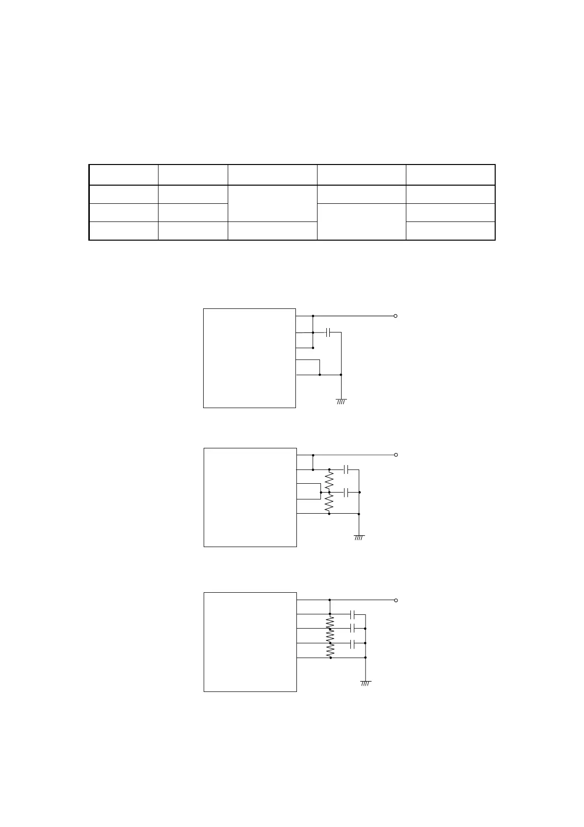
<1> In the case of generating the drive voltage outside the LSI
Supply each voltage described in Table:17.3.2 to VLC1, VLC2 and VLC3.
Figure:17.3.1 shows the connection with the external resistors, and each capacitor should be 0.1 µF.
Table:17.3.2 Voltage level of VLC1/VLC2/VLC3
V
LCD
: LCD drive voltage, the maximum voltage supplied to LCD panel.
Figure:17.3.1 Connection Examples of LCD Power Supply
(when using external voltage dividing resistor)
Pin Name Voltage Level Static 1/2-bias 1/3-bias
VLC1 V
LC1
V
LCD
+ V
SS
V
LCD
+ V
SS
V
LCD
+ V
SS
VLC2 V
LC2
1/2V
LCD
+ V
SS
2/3V
LCD
+ V
SS
VLC3 V
LC3
V
SS
1/3V
LCD
+ V
SS
VLC1
VLC2
VLC3
VSS
VDD30
VLC1
VLC2
VLC3
VSS
VDD30
DD30
LCD
b)1/2duty,1/2bias(VDD30 = VLCD)
R
R
C
C
C
c)1/3duty to 1/8duty 1/3bias(VDD30 = VLCD)
R
R
R
VLC1
VLC2
VLC3
VSS
VDD30
C
C
C
VDD30 inp
VDD30 inp
VDD30 inp
 Loading...


