S3F84B8_UM_REV 1.00 1 OVERVIEW OF S3F84B8 MICROCONTROLLER
1-8
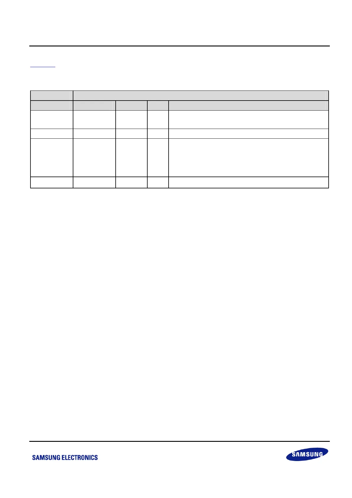
Table 1-2 shows the pin descriptions used to Read/Write the Flash ROM in S3F84B8.
Table 1-2 Pin Descriptions used to Read/Write the Flash ROM
Main Chip During Programming
Pin Pin Name Pin No. I/O Function
P2.6 SDA 18 I/O Serial data pin (output when reading, Input when writing)
Input and push-pull output port can be assigned
P2.7 SCL 19 I Serial clock pin (input only pin)
RESET/P0.2 VPP 4 I Power supply pin for flash ROM cell writing (indicates that
MTP enters into the writing mode). When 11 V is
applied, MTP is in the writing mode and when 5 V is
applied,
MTP is in the reading mode. (Optional)
V
DD
/V
SS
V
DD
/V
SS
20/1 I Logic power supply pin.



 To Next Page