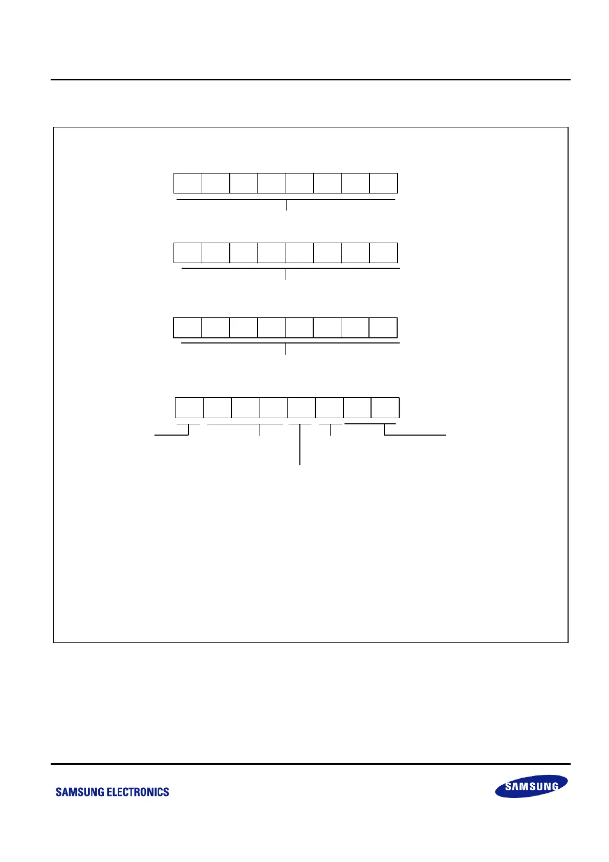
S3F84B8_UM_REV 1.00 2 ADDRESS SPACES
2-3
2.2.1 SMART OPTION
NOTE:
1. The unused bits of 3CH, 3DH, 3EH, 3FH must be logic "1".
2. When LVR is enabled, LVR level must be set to appropriate value .
3. P0.2 has only input (without pull-up) function when sets 003F.2 as 0.
4. You must set P0.0,P0.1,P0.2 function on smart option. For example, if you select XIN (P0.0)/XOUT (P0.1)/nRESET(P0.2)
function by smart option , you can’t change them to Normal I/O after reset operation.
LVR enable
or disable bit:
0=Disable
1=Enable
LVR level selection
101 = 1.9 V
110 = 2.3 V
100 = 3.0 V
001 = 3.6V
011 = 3.9 V
ROM Address: 003FH
.7 .6 .5 .4 .3 .2 .1 .0MSB LSB
Not used
P0.2/nRESET pin
selection bit:
0 = P0.2 pin enable
1 = nRESET
Pin enable
Oscillation selection bit:
00 = External crystal (Xin/Xtout pin
enable)
01 = External RC(Xin/Xtout pin enable)
10 = Internal oscillator (0.5MHz)
(P0. 0, P0.1 are normal IOs)
11 = Internal oscilator (8MHz)
(P0. 0, P0.1 are normal IOs)
ROM Address: 003CH
.7 .6 .5 .4 .3 .2 .1 .0MSB LSB
ROM Address: 003DH
.7 .6 .5 .4 .3 .2 .1 .0MSB LSB
Not used
Not used
ROM Address: 003EH
.7 .6 .5 .4 .3 .2 .1 .0MSB LSB
Not used
Figure 2-2 Smart Option
For Start condition of the chip, Smart option specifies the ROM option. The ROM address used by Smart option is
from 003EH to 003FH. Note that 003CH and 003DH are not used in S3F84B8.