S3F84B8_UM_REV 1.00 13 A/D CONVERTER
13-3
13.1.2 INTERNAL REFERENCE VOLTAGE LEVELS
In the ADC function block, the analog input voltage level is compared to the reference voltage. The reference
voltage is internally connected to VDD in S3F84B8. Thus, the analog input level must remain within the range of
V
SS
to V
DD.
Different reference voltage levels are generated internally along the resistor tree during the analog conversion
process for each conversion step. The reference voltage level for the first bit conversion is always 1/2 V
DD.
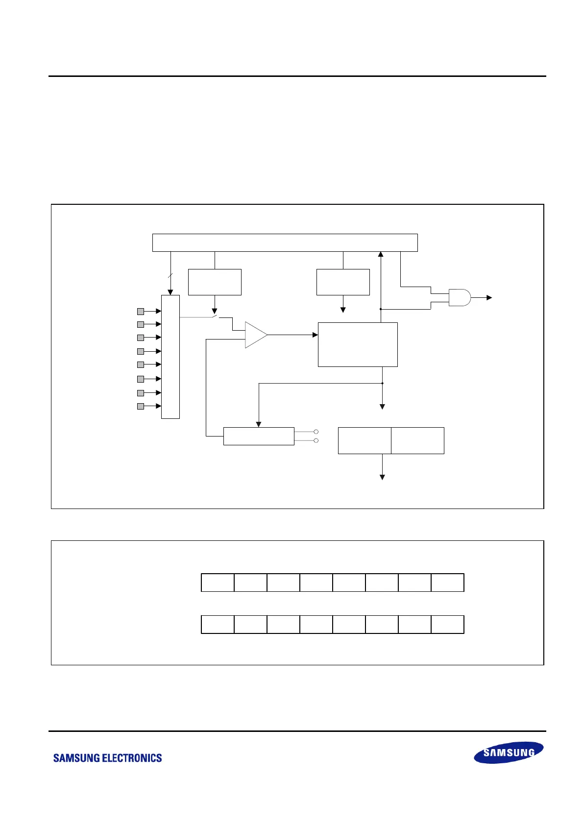
A/D Converter Control Register
ADCON (FAH)
ADCON.7-.5
M
U
L
T
I
P
L
E
X
E
R
Control
Circuit
+
-
D/A Converter
V
DD
V
SS
Successive
Approximation
Circuit
Analog
Comparator
Clock
Selector
ADCON.0 (ADEN)
ADCON.2-.1
Conversion Result
ADDATAH
(F8H)
ADDATAL
(F9H)
To data bus
ADCON.3
(pending)
ADC0/P0.0
ADC1/P0.1
ADC2/P0.2
ADC7/P0.3
ADC8/P0.4
ADC2/P0.5
ADC7/P0.6
ADC8/P0.7
ADCON.4
ADINT
Figure 13-2 A/D Converter Circuit Diagram
LSBMSB .7 .6 .5 .4 .3 .2 .1 .0
- --- .1.0MSB LSB
ADDATAH
ADDATAL
--
Figure 13-3 A/D Converter Data Register (ADDATAH/L)
 Loading...