S3F84B8_UM_REV 1.00 4 CONTROL REGISTERS
4-31
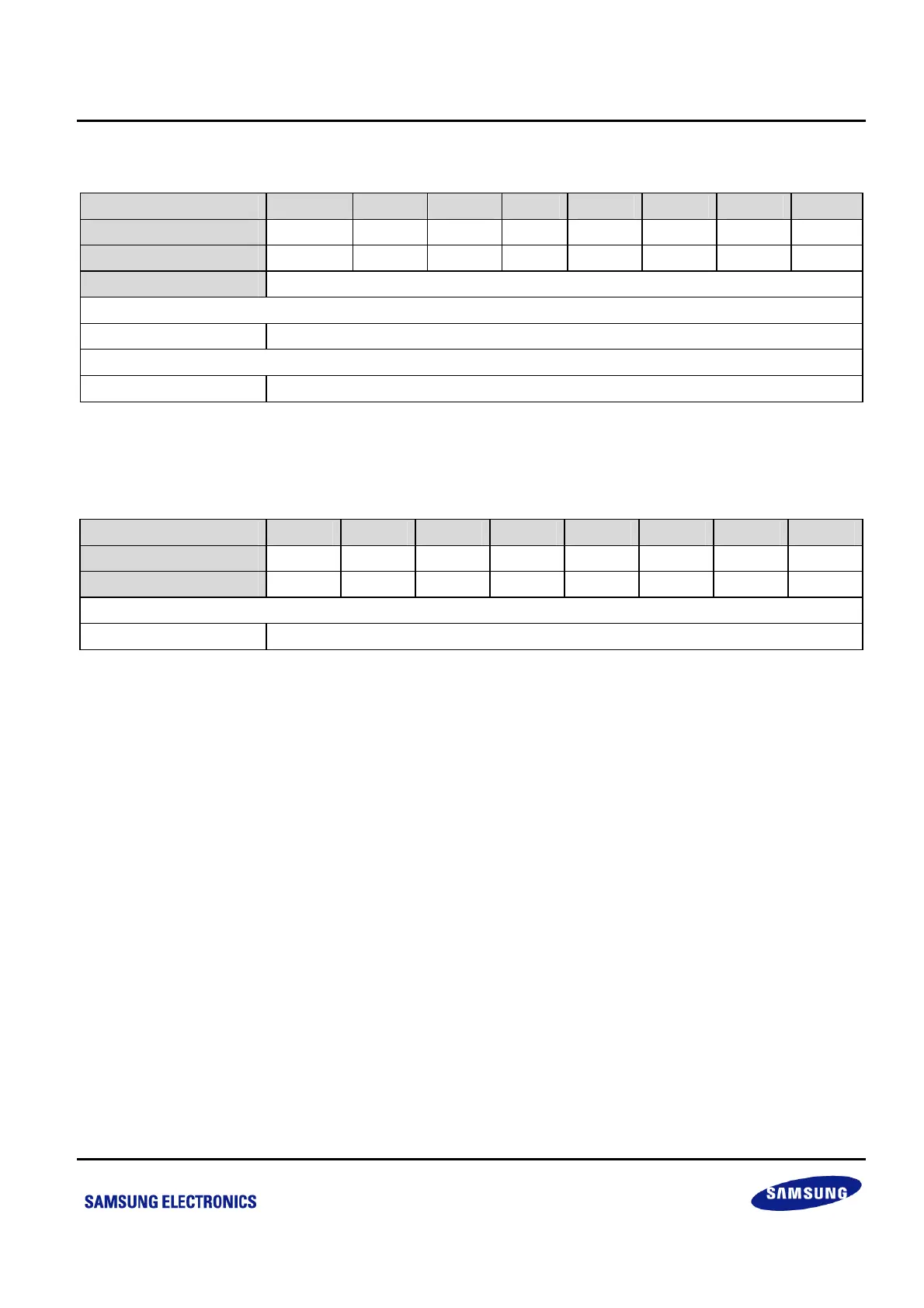
4.1.31 PWMDL — COMPARATOR0 OUTPUT DELAY REGISTER: F5H, BANK0
Bit Identifier .7 .6 .5 .4 .3 .2 .1 .0
RESET Value
– – – – 0 0 0 0
Read/Write
– – – – R/W R/W R/W R/W
Addressing Mode
Register addressing mode only
.7–.4 Not used for S3F84B8.
.3–.0
Delay Time = (PWMDL+1)4/fpwmclk + TST
NOTE: 0 < TST(setting time)< 4/fpwmclk
4.1.32 PP — REGISTER PAGE POINTER: DFH, BANK0
Bit Identifier .7 .6 .5 .4 .3 .2 .1 .0
Reset Value
0 0 0 0 0 0 0 0
Read/Write
R/W R/W R/W R/W R/W R/W R/W R/W
.7–.0 Not used for S3F84B8.
NOTE: In S3F84B8, only Page 0 settings are valid. Register page pointer values for the source and destination register page
are automatically set to ‘00F’ following a hardware reset. These values should not be changed during normal
operation.