S3F84B8_UM_REV 1.00 21 ELECTRICAL DATA
21-9
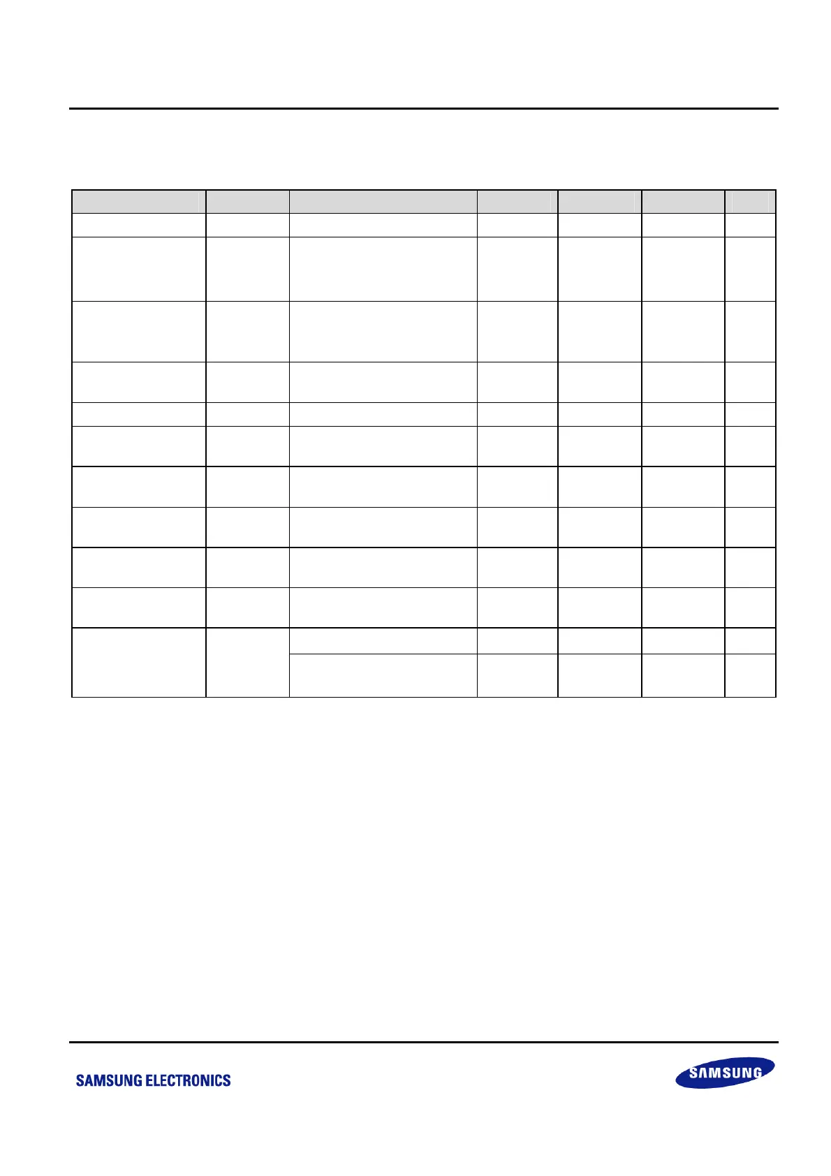
Table 21-7 A/D Converter Electrical Characteristics
(T
A
= –40C to + 85C, V
DD
= 1.8V to 5.5V, V
SS
= 0V)
Parameter Symbol Test Conditions Minimum Typical Maximum Unit
Resolution – 10 – bit
Total accuracy
V
DD
= 5.12V
(1)
CPU clock = 10MHz
V
SS
= 0V
– –
3
LSB
Integral linearity
error
ILE – – –
2
LSB
Differential linearity
error
DLE – – –
1
LSB
Offset error of top EOT – –
1 3
LSB
Offset error of
bottom
EOB – –
1 3
LSB
Conversion
time
(2)
t
CON
– 12.5 20
s
Analog input
voltage
V
IAN
–
V
SS
–
V
DD
V
Analog input
impedance
R
AN
– 2 1000 –
M
Analog input
current
I
ADIN
V
DD
= 5V
– – 10
A
V
DD
= 5V
– 0.5 1.5 mA
Analog block
current
(3)
I
ADC
V
DD
= 5V
Power down mode
100 500 mA
NOTE:
1. When V
DD
= 2.7V to 5.5V, the total accuracy is characterized to be maximum 3LSB, but not tested.
2. “Conversion time” specifies the time required from the moment a conversion operation starts until it ends.
3. I
ADC
specifies the operating current during A/D conversion.



 To Next Page