S3F84B8_UM_REV 1.00 4 CONTROL REGISTERS
4-15
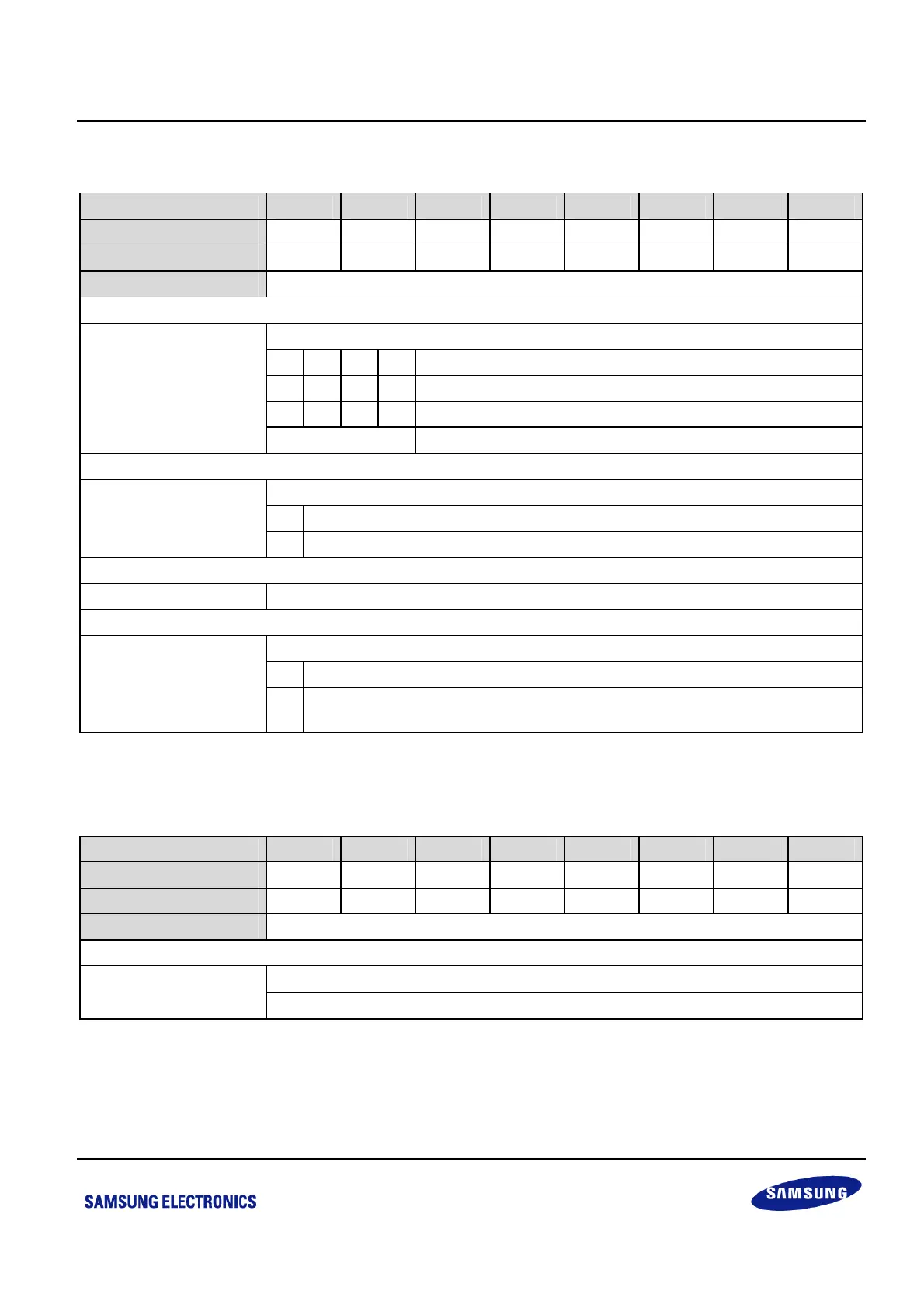
4.1.12 FMCON — FLASH MEMORY CONTROL REGISTER: F5H, BANK1
Bit Identifier .7 .6 .5 .4 .3 .2 .1 .0
Reset Value
0 0 0 0 0 – – 0
Read/Write
R/W R/W R/W R/W R – – R/W
Addressing Mode
Register addressing mode only
Flash Memory Mode Selection Bits
0 1 0 1 Programming mode
1 0 1 0 Sector erase mode
0 1 1 0 Hard lock mode
.7–.4
Other values Not available
Sector Erase Status Bit
0 Success sector erase
.3
1 Fail sector erase
.2–.1 Not used for the S3F84B8
Flash Operation Start Bit
0 Operation stops.
.0
1 Operation starts (This bit will be cleared automatically just after the
corresponding operation is completed).
4.1.13 FMSECH — FLASH MEMORY SECTOR ADDRESS REGISTER (HIGH
BYTE): F7H, BANK1
Bit Identifier .7 .6 .5 .4 .3 .2 .1 .0
Reset Value
0 0 0 0 0 0 0 0
Read/Write
R/W R/W R/W R/W R/W R/W R/W R/W
Addressing Mode
Register addressing mode only
Flash Memory Sector Address Bits (High Byte) .7–.0
The 15
th
- 8
th
bits selects a sector of flash ROM.
NOTE: The high byte Flash Memory Sector Address Pointer’s value is the higher 8-bits of the 16-bit pointer address.