S3F84B8_UM_REV 1.00 4 CONTROL REGISTERS
4-6
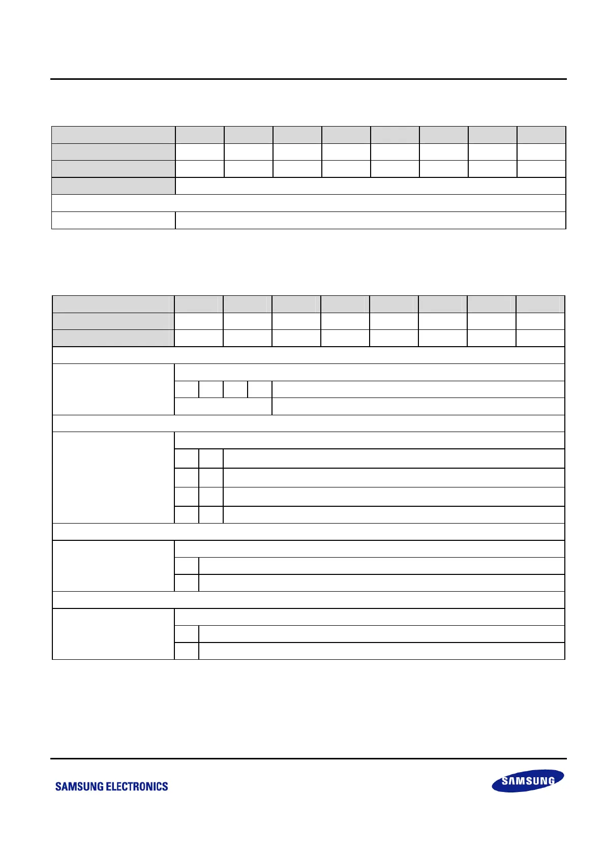
4.1.2 AMTDATA — ANTI-MIS-TRIGGER DATA REGISTER: F6H, BANK0
Bit Identifier .7 .6 .5 .4 .3 .2 .1 .0
RESET Value
0 0 0 0 0 0 0 0
Read/Write
R/W R/W R/W R/W R/W R/W R/W R/W
Addressing Mode
Register addressing mode only
.7–.0
Anti-mis-trigger time= (AMTDATA 4)/fpwmclk + TST
NOTE: 0 < TST (setting time) < 4/fpwmclk
4.1.3 BTCON — BASIC TIMER CONTROL REGISTER: D3H, BANK0
Bit Identifier .7 .6 .5 .4 .3 .2 .1 .0
RESET Value
0 0 0 0 0 0 0 0
Read/Write
R/W R/W R/W R/W R/W R/W R/W R/W
Watchdog Timer Function Enable Bit
1 0 1 0 Disables watchdog timer function.
.7–.4
Others Enables watchdog timer function.
Basic Timer Input Clock Selection Code
0 0
f
OSC
/4096
0 1
f
OSC
/1024
1 0
f
OSC
/128
.3–.2
1 1 Invalid setting
Basic Timer 8-Bit Counter Clear Bit
0 No effect.
.1
1 Clears the basic timer counter value.
Basic Timer Divider Clear Bit
0 No effect.
.0
1 Clears both the dividers.
NOTE: When you write a “1” to BTCON.0 (or BTCON.1), the basic timer divider (or basic timer counter) is cleared. The bit is
then automatically cleared to “0”.
 Loading...